Some great analysis on SSD wear leveling and power consumption

Some great analysis by Cullen Logan at Amazon.com appeared on LinkedIn over the weekend in response to my post “Are Enterprise SSDs a “bad” idea? Four tips and counter-tips for your consideration”:

“To put some raw data out there, consider a single 8Gb MLC NAND with 4096 blocks. If a naive approach were taken that performs an ERASE/REPROGRAM every minute, the typical 10,000 cycle limit would be reached in just 7 days (60 x 24 x 7 = 10,080 = good-bye block).

But as Steve points out there are really smart people working on this stuff. Using a perfect wear-leveling scenario that evenly distributes ERASE/REPROGRAM cycles across all 4096 blocks would result in each block being written a maximum of 3 times in that 7 day period 10,080/4096 = ~2.46. Put another way, wear leveling can extend the life of the MLC NAND to over 77 years using this simplistic example.

(10,000 x 4096)/(60×24) = 28,444 days = ~77.87 years

Other topics that should be considered is whether or not the controller utilizes partial page writes (which increases read disturbances), background operations, and many other features defined in JEDEC specs for eMMC – although eMMC is not exactly the same as SSD; they share many things in common.

While some anecdotal comments in this thread suggest that power is not something to consider with SSDs, I tend to disagree. As bus frequencies increase we must compensate by attempting to lower the voltage supplied, to help the overall power equation. In that equation voltage is squared, so any reduction in voltage is a big win. Lowering the voltage on HDDs is a larger hurdle due to mechanical parts, while wafer processing tends to lean in favor for SSDs and required voltage.

I could probably write for another hour about this, but my meta-point is that SSDs are in no way bad. As Steve mentioned ECC selection will need to evolve or perhaps become application dependent, which will result in extra bits per block, but will provide the right ECC for an application’s target BER.

My only complaint is the lack of transparency in the methods used by controller vendors in how exactly they manage bad blocks. It makes robust testing nearly impossible if not done in an oven, and even then you can’t get raw data on block failures, because the controller takes care of it by design and how it does so is secret sauce for the controller vendor.

SSDs are here to stay. Any enterprising company will have backup measures in place already for critical and perhaps non-critical data, so price will probably be a large determining factor for large-scale corporate purchases. Just my $0.02.

Thanks Steve for a great post to generate some activity.”

Posted by Cullen Logan.

Thanks, Cullen!

Posted in NAND, SSD | Tagged , , , , , | Leave a comment

The Economist covers PCM – must be something real

I was surprised to see an article about phase-change memory (PCM) appear early this month in the well-respected British magazine The Economist. “Altered states” provides a good, basic introduction to PCM.

Posted in PCM | Tagged , , | Leave a comment

Add OCZ to the growing list of SSD vendors differentiating their drives with a proprietary controller

SSD vendor OCZ has been showing its new top-of-the-line Vector 2.5-inch SSD at this week’s Intel Developers Forum in San Francisco. During a conference call with analysts, OCZ CEO Ryan Peterson reportedly discussed the controller in the new SSD. It’s the Indilinx Barefoot 3, an all-new design internally developed by OCZ, which bought controller vendor Indilinx last year.

Many SSD vendors have been acquiring SSD controller vendors or developing in-house SSD controllers as a way to differentiate their storage products.

For more discussion of this topic, see:

Using SSD controller technology as a differentiator: Kingston adds another data point with SSDNow Enterprise-class drives

Need yet another argument for designing your own SSD controller?

Add Hitachi Data Systems to the growing list of companies developing their own SSD controllers

How Skyera developed the 44Tbyte, enterprise-class Skyhawk SSD from the ground up. A System Realization story.

More on developing your own SSD controller chip. Is rolling your own right for you?

STEC’s MACH16 Slim 2.5-in SATA SSD requires small footprint, fits in small embedded spaces

Micron introduces Enterprise-class, 2.5-inch SSD with PCIe interface

Examining The SSD Industry – Researching The Controller or Processor

Posted in Uncategorized | Leave a comment

IDT announces DDR4 register chip for DDR4 registered DIMMs and 3D die stacks

IDT has announced a small but essential component for the development of advanced DDR4 DIMMs: the 4RCD0124 DDR4 register. A device of this type is required for building DDR4 DIMMs to provide registered buffering. In addition, the 4RCD0124 DDR4 register includes advanced RAS (reliability, availability, and serviceability) features and support for 3D SDRAM die stacking on the DIMM.

Posted in DDR4, SDRAM | Tagged , | Leave a comment

Western Digital sampling 5mm, 2.5-inch, 500Gbyte hybrid HDD with NAND Flash

Western Digital just started shipping 7mm, 2.5-inch HDDs earlier this year and has now announced that it is sampling a 5mm, 2.5-inch, 500Gbyte hybrid HDD with integrated NAND Flash caching. The drive will be showcased during Western Digital’s Investor Day on September 13. The announcement quotes spokespeople from both Acer and Asus, two of the leading PC notebook vendors that appear to be collaborating with Western Digital on the slimmer drive, which is clearly targeted at Ultrabook designs. As the announcement points out, the 5mm drive consumes a little more than half of the volume of a 9.5mm drive, which is important for Ultrabooks because of the small form factor.

Posted in Flash, HDD, SSD | Tagged , , , , , | Leave a comment

Will the Apple iPhone 5 use PCM?

An investment site called Seeking Alpha has published a bit of strange forensic research that leads it to claim that the Apple iPhone 5 that will be announced tomorrow employs phase-change memory (PCM). What clue led to this conclusion? It was the mention of PCM in a US patent application filed early last year on January 14, 2011, number 20120185797.

Part of the patent application’s description reads:

“[0023] The data processing system 100 includes memory 110 which is coupled to the microprocessor(s) 105. The memory 110 may be used for storing data, metadata, and programs for execution by the microprocessor(s) 105. The memory 110 may include one or more of volatile and non-volatile memories, such as Random Access Memory (“RAM”), Read Only Memory (“ROM”), Flash, Phase Change Memory (“PCM”), or other types of data storage.”

Now this is a real stretch of the imagination if you know how all inclusive companies try to make patent applications. Nevertheless, Micron recently introduced a combo SDRAM/PCM product—see “3D Thursday: Micron stacks Phase-Change Memory and SDRAM”—although the amount of PCM in that product isn’t enough to hold an iPhone’s operating system.

So could the new Apple iPhone 5 contain PCM? It’s certainly not impossible. I guess we just have to wait until tomorrow to find out.

Posted in PCM | Tagged , , , | Leave a comment

IBM gets patent for hi-temp PCM (phase-change memory) cell structure

Tom’s Hardware is reporting that IBM recently obtained a patent on specially formulated phase-change memory (PCM) that will operate above 150°C. This is a significant achievement because PCM has a problem with ambient thermal annealing. If the chip temperature goes too high, then the phase-change memory cells will start to self erase as they change from their amorphous state to a crystalline state. This was not a problem for the recently announced LPDDR2 PCM/SDRAM combo device from Micron. (See “3D Thursday: Micron stacks Phase-Change Memory and SDRAM”) I know it’s not a problem for the device’s 0-85°C temperature range because I asked about that problem. Operating at more than 150°C is yet another story entirely.

Posted in PCM, Storage | Tagged , , | Leave a comment

Future Memory: The MemCon Panel. What comes after NAND Flash and DRAM?

Just announced, there’s a pre-lunch panel at MemCon covering future memories. There are several new memory technologies that would usurp the thrones from DRAM and NAND Flash memory. Will any succeed? Come and hear the panel to find out.

Jim Handy, “The Memory Guy” and Chief Analyst at Objective Analysis will moderate. The panelists include:

  • Christophe Chevallier, Vice President, NVM/Storage Division, Rambus
  • Barry Hoberman, Chief Marketing Officer, Crocus
  • Michael Miller, Vice President, Technology, Innovation and Systems Applications, MoSys

MemCon is a free event, taking place on September 18 at the Santa Clara Convention Center. Breakfast, lunch, and an Octoberfest early evening celebration are also free, so sign up here.

Posted in DRAM, Flash, MRAM, NAND | Tagged , , , | Leave a comment

Using SSD controller technology as a differentiator: Kingston adds another data point with SSDNow Enterprise-class drives

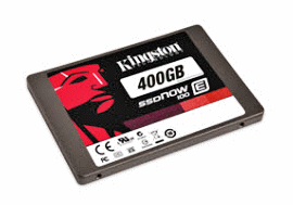
Kingston E100 SSD

Memory and SSD vendor Kingston Technology has just announced enterprise-class SSDs called the SSDNow E100 in capacities of 100, 200, and 400 Gbytes. What I find interesting about this announcement are the emphasis on endurance and reliability (“10x improvements … over client SSDs”) and the use of special names for endurance enhancements (DuraWrite) and reliability (RAISE). What’s notable about these two terms is that they are leveraged from LSI SandForce, which supplies the SSD controller chip for these drives.

According to SandForce, DuraWrite “optimizes the number of program cycles to the flash effectively extending flash rated endurance by 20x or more when compared to standard controllers” and RAISE (Redundant Array of Independent Silicon Elements) “deliver an orders-of-magnitude improvement in drive reliability versus today’s best enterprise HDDs and SSDs. The result is single-drive RAID-like protection and recovery from a potentially catastrophic flash block failures – all while avoiding the inefficiencies of traditional RAID.”

What I think is notable here is that Kingston, which has an excellent reputation in this industry already, is relying on SandForce controller technology and terminology to carry the water for the SSDNow drives’ endurance and reliability.

For more discussion of this topic, see:

Need yet another argument for designing your own SSD controller?

Add Hitachi Data Systems to the growing list of companies developing their own SSD controllers

How Skyera developed the 44Tbyte, enterprise-class Skyhawk SSD from the ground up. A System Realization story.

More on developing your own SSD controller chip. Is rolling your own right for you?

STEC’s MACH16 Slim 2.5-in SATA SSD requires small footprint, fits in small embedded spaces

Micron introduces Enterprise-class, 2.5-inch SSD with PCIe interface

Examining The SSD Industry – Researching The Controller or Processor

Posted in SSD, Storage | Tagged , , , , , | 1 Comment

It’s what you do with the memory that counts. Case in point: the TI Stellaris M4F microcontrollers

NAND Flash wear leveling is an established error- and fault-management technique in SSDs, but Texas Instruments is touting on-chip Flash and EEPROM durability in a low-cost microcontroller: the TI Stellaris M4F series based on the ARM Cortex-M4F microprocessor core. There’s a 256Kbyte Flash memory on the TI Stellaris M4F microcontroller. Here are the relevant words TI uses to describe the Flash memory on the device:

“It can be hard to get excited about memory. It is often simply taken for granted. But changing to a TI 65nm process for the Stellaris LM4F family raises the products to a new level of reliability and integration. Borrowing the Flash technology that TI developed for use in automotive products, the Stellaris LM4F MCUs have extended memory durability by an order of magnitude beyond competition. The minimum number of times the flash memory on these MCUs can be erased and reprogrammed is as high as 100,000 cycles.

For most applications, this breakthrough eliminates any concern of wearing out the memory from re-flashing for data collection, configuration parameters or program modifications. More of the high-reliability Flash is also available for customer-written code because StellarisWare drivers are embedded in a small mask ROM on-chip.

All Stellaris LM4F MCUs have the StellarisWare binaries committed in on-chip ROM, including the peripheral drivers, the in-system programming routines, utilities such as CRC (cyclic redundancy check) algorithms, and AES (advanced encryption standard) tables. These APIs (application programming interfaces) let the programmer take full advantage of these well-proven services, routines and tables, while leaving all of the flash for customer and application-specific code.”

There’s also a 2Kbyte EEPROM on the TI Stellaris microcontroller, described like this:

“There are many other memory features on the MCUs, but one new memory type deserves special attention. The new Stellaris LM4F MCUs have 2K bytes of secure, on-chip EEPROM. EEPROM is normally used to store long-term variables that may even need to survive power outages and dead batteries. Since the implementation is interrupt-enabled, the integrated memory allows for the execution of code while writing values to nonvolatile memory (execute-while-write). The EEPROM use is architected using a built-in wear- leveling technique that ensures each location can be modified 500,000 times. If the data was re-written 100 times a day, the EEPROM would last nearly 15 years!”

Make no mistake. Memory is a very competitive part of any SoC or system design, no more and no less important that other components. Memory is not as simple as it might seem at first and the right approach to providing memory in a design can make a big difference in its perceived value.

For more information on the TI Stellaris M4F microcontroller and its new eval board, see “TI Stellaris LaunchPad eval board features ARM Cortex-M4F. Intro price: $4.99. Get yours now.

Posted in ARM | Tagged , , , , | Leave a comment

How ya gonna’ control that DDR4 SDRAM next year? The 28nm answer.

Cadence has just completed testing of its DDR4 SDRAM controller and PHY in two of the TSMC 28nm process technologies: 28HPM and 28HP. The DDR4 PHY exceeds the data rates needed to operate DDR-2400 SDRAMs and it is interoperable with DDR3 and DDR3L SDRAM devices as well. The same test chip also included an all-digital mobile SDRAM PHY capable of DDR-1600 and DDR-1833 DDR3 data rates and full-speed LPDDR2 SDRAM data rates as well. In addition, the test chip included a copy of the Cadence DDR4 SDRAM controller, so that too is now silicon proven.

Although the JEDEC DDR4 SDRAM specification is still in draft form, it’s expected in final form later this year. Production SDRAM devices based on this standard will follow shortly after finalizing the spec, as evidenced by early prototype announcements from Micron and Samsung. You can expect to see the first products based on DDR4 memory to begin appearing next year.

For more information on DDR4, see:

The DDR4 SDRAM spec and SoC design. What do we know now?

and

Memory to processors: ‘Without me, you’re nothing.’ DDR4 is on the way.

For more information on the Cadence announcement, see “Cadence Announces Industry’s First DDR4 Design IP Solutions Are Now Proven in 28nm Silicon.”

Posted in DDR, DDR3, DDR4, DRAM, LPDDR2, SDRAM | Tagged , , , , , , , | Leave a comment

The top 21 things you probably didn’t know about Flash memory, from the Flash Memory Summit

Last week’s Flash Memory Summit ended with a session titled “The top 10 things you need to know about Flash memory today. Richard Goering summarized the panel in his blog titled “Flash Memory Panelists Challenge Conventional Thinking About NAND and SSDs” but I thought it would be fun to compile that information into a longer list. So for your amusement, here are the top 21 things you don’t know about Flash memory based on presentation from Andy Tomlin, VP of Solid state Development at Western Digital; Jered Floyd, CTO of Permabit; and Jim Handy, Chief Analyst at Objective Analysis:

  1. It takes a minimum of two years to develop firmware for a new SSD and if you think it takes less, you’ll make poor decisions along the way. –Tomlin
  2. Flash is already cheaper than disk. –Floyd
  3. Data optimization is a requirement. –Floyd
  4. You shouldn’t build it yourself. –Floyd
  5. The end of the road is not in sight. –Floyd
  6. Enterprise is a quality grade, not a technology. –Floyd
  7. Flash device vendors will vertically integrate—or die. –Floyd
  8. Hybrid drives are nothing new. –Floyd
  9. Consumers will be all flash. –Floyd
  10. Data centers will all adopt Flash. –Floyd, Handy
  11. Flash will save the world. –Floyd
  12. NAND prices will not rebound until mid 2013. –Handy
  13. New controllers will enable enterprise-class SSDs based on TLC Flash. –Handy
  14. NAND-aware software is the next high-growth market. –Handy
  15. Ultrabooks will drive NAND Flash cache use in PCs and notebooks. –Handy
  16. The SSD market will split into multiple segments. –Handy
  17. Alternative (new) memories will displace very little NOR Flash. –Handy
  18. PC SSD revenues will decline with the adoption of Flash cache. –Handy
  19. Few will realize it when Flash reaches its scaling limit. –Handy
  20. The current SSD form factor and interface will eventually disappear. –Handy
  21. Flash will eventually scale to 10nm and then be replaced in 6 to 8 years. –Handy
Posted in Flash, SSD, Storage | Tagged , , , , , , , | Leave a comment

Need yet another argument for designing your own SSD controller?

A Web site called legitreviews.com recently reviewed the ADATA XPG SX900 128Gbyte SSD and this review contains additional justification for seriously considering developing your own SSD controller for new storage products. The review starts off this way:

“ADATA is long known for their memory and storage products and as such, are well known even outside of tech circles. They’ve stepped a bit on the ledge with the marketing of their SX900 series of drives with ‘the most powerful SSD on Earth’ prominently displayed on the product page of their website. Being that this is yet another SandForce (LSI) SF-2281 drive with what appears to be relatively generic firmware, this appears to be more hype than substance. Still, we took it upon ourselves to give the 128GB version they sent us a good working over to see what all the fuss was about.”

The review quickly gets into a discussion of the drive’s internals and this is what the authors have to say:

“Once again we find ourselves looking upon the ever popular SandForce (LSI) SF-2281 SSD controller which nearly everyone that has been even remotely following SSDs should be familiar with. Employing real time compression technology, they are essentially able to turbocharge writes and post some impressive numbers. We also know that it does a nice job at wear-leveling, encryption and supports TRIM as well as idle garbage collection. There’s a good reason why this controller shows up in drives from nearly every manufacturer – it’s a solid performer.”

And so the review’s conclusion should not come as a surprise:

“In the opening of the article, we made reference to ADATA’s marketing of the SX900 as the “most powerful SSD on Earth” and after spending some time banging on the drive do we feel that description is warranted? Nope. It’s really more or less equal to a fair number of drives on the market already.”

My conclusion: the SSD controller and the controller firmware are key differentiators for many—certainly for these reviewers. The Denali Memory Report has already written about several companies that either are or are planning on developing their own SSD controllers and they are doing this work specifically for differentiation in the marketplace.

For more discussion of this topic, see:

Add Hitachi Data Systems to the growing list of companies developing their own SSD controllers

How Skyera developed the 44Tbyte, enterprise-class Skyhawk SSD from the ground up. A System Realization story.

More on developing your own SSD controller chip. Is rolling your own right for you?

STEC’s MACH16 Slim 2.5-in SATA SSD requires small footprint, fits in small embedded spaces

Micron introduces Enterprise-class, 2.5-inch SSD with PCIe interface

Examining The SSD Industry – Researching The Controller or Processor

Posted in SSD, Storage | Tagged , , , , , , , | 2 Comments

What does Intel’s choice of GDDR5 graphics DRAM for main memory with its Manycore Xeon Phi coprocessor say about SoC design?

George Chrysos discussed the Intel MIC (Many Integrated Core) architecture of the Knights Bridge chip (officially called the Intel Xeon Phi coprocessor) at today’s Hot Chips 24 conference and disclosed that it uses GDDR5 graphics memory as the main memory for the manycore part. In fact, the Intel Xeon Phi coprocessor has several (an undisclosed number) on-chip GDDR5 memory controllers. Now GDDR5 SDRAM is high-bandwidth memory generally found on graphics cards, not computing engines. GDDR5 memory supports extremely high data rates in the tens of Gbits/sec using multi-GHz transfer clocks. These SDRAMs also cost more per Gbit than bulk SDRAM, but you’re paying for performance.

And memory performance is exactly what the Intel Xeon Phi coprocessor requires because it contains more than 50 x86 processor cores with an immense thirst for data. Slaking that thirst is why Intel selected GDDR5 graphics SDRAM.

I think this choice has implications for many future manycore SoC designs. The Intel Xeon Phi coprocessor gives us a taste of things to come with other manycore SoC designs. Although the Intel Xeon Phi coprocessor is a homogeneous computing device, the same memory bandwidth issues will surround multicore heterogeneous SoC designs as well. However, I doubt that the solution for these designs will be the use of GDDR5 SDRAM, because that’s not a low-cost approach. Intel can afford to use expensive, high-performance SDRAM because the application, server-centric HPC (high-performance computing), warrants the expense. The Intel Xeon Phi coprocessor replaces even more expensive computing clusters. However most SoCs will need a different sort of approach that doesn’t cost as much.

Wide I/O SDRAM is one possibility, but it requires a more mature 3D IC assembly infrastructure. The Hybrid Memory Cube Consortium represents another such approach, but its target application is HPC, the same application targeted by the Intel Xeon Phi coprocessor.

It’s a problem that will need solving.

For more information on the Intel Xeon Phi coprocessor, see “Zowie! More than 50 x86 cores on the Intel Knights Corner Manycore Coprocessor

For more information on Wide I/O SDRAM, see “Wide I/O. Don’t leave your SoC without it

For more information on the Hybrid Memory Cube, see:


Posted in DDR, HMC, Hybrid Memory Cube, SDRAM | Tagged , , , , , | 1 Comment

Want to know why SK hynix is placing its bets on three different alternatives to DRAM and Flash?

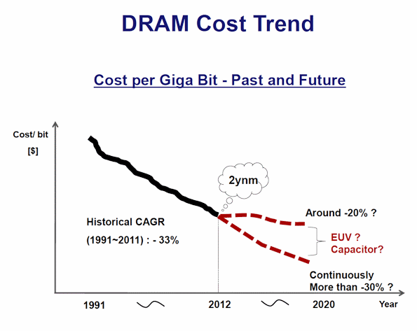
Last week at the Flash Memory Summit, Dr. Sung Wook Park spoke about memory. No surprise there, but there were several surprises in Park’s presentation. The first surprise popped up in the slide immediately following the keynote presentation’s title slide:

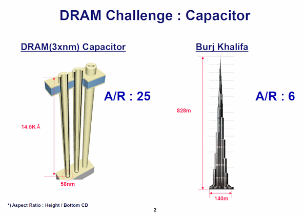
From Park’s perspective, the 33% per year compound annual decline in DRAM cost per bit is about to end at the low 20nm side of the scaling equation (2ynm in the slide). After that, there are some pretty large scaling problems to be overcome and Park didn’t sound optimistic about overcoming them. The reason for his pessimism appeared on the very next slide:

The aspect ratio of the deep capacitors used to store digital bits as charge in DRAMs has gotten ludicrous. The capacitor’s aspect ratio is now at 25. The aspect ratio of the Burj Khalifa, which is currently the tallest human artifact in the world, is only 6. The current capacitor design needs re-engineering or DRAM scaling’s going to slow down significantly.

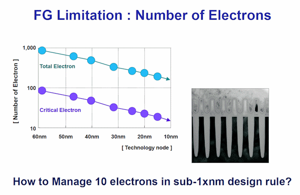
NAND Flash is also running into trouble, in the form of the dwindling number of electrons stored in the NAND Flash cell’s floating gate as the gate’s volume shrinks with each process node.

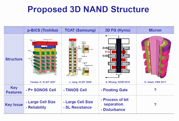
The number of electrons stored in the NAND Flash cell’s floating gate is rapidly headed towards a couple of hundred and there’s a signal/noise problem were the leakage loss of even 10 electrons is becoming problematic. Consequently, there’s a quest for developing 3D NAND Flash cell structures, which greatly expand the volumetric capacity of the bit cell’s floating gate. Park showed a slide with four proposed 3D NAND cell designs from Toshiba, Samsung, SK hynix, and Micron.

For these reasons, SK hynix (and other semiconductor memory vendors) are ramping their search efforts to find replacement technologies for DRAM and NAND Flash. As I’ve written before (see “SK hynix places bet on third wannabe non-volatile memory technology, phase-change memory, with IBM”), SK hynix is pursuing Phase-Change Memory (PCM) with IBM, MRAM (magnetic RAM) with Toshiba, and memristors (resistive RAM or ReRAM) with HP.

Park said that any such memory replacement technology must satisfy at least one of the following:

  • Drop-in replacement (pin-for-pin compatible)
  • Better cost and power than DRAM.
  • Better reliability and performance than NAND Flash memory.

Whatever the replacement memory technology turns out to be, said Park, it must also offer byte-level accessibility.

PCM is the most mature at the moment, said Park. It combines the advantages of Flash and DRAM. It’s still expensive. Nevertheless, there’s a successfully manufactured 1Git, PCM 42nm device and a 2xnm PCM cell structure is in development.

Then Park said that MRAM still needs work. Although MRAM is promising because the cell structure is close to the size of a DRAM cell, there are “still many challenges.”

Finally, said Park, memristors are “still a ways away.” “We need a better understanding of the underlying mechanism and its reliability,” he explained.

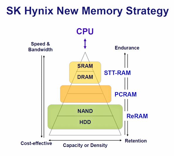
With all of these caveats, one of Park’s final slides showed that SK hynix has found a place for each of these three wannabe memory technologies in a system:

Park’s slide shows SRAM and DRAM being replaced with STT-MRAM (STT stands for “spin-torque transfer). PCM or ReRAM could be a possible replacement for NAND Flash and hard disk drives. PCM (PCRAM) appears to fall into a currently unpopulated memory niche between DRAM and NAND Flash memory. These positions in the memory hierarchy are based on the respective cost, bit-density, and performance characteristics of the prospective memory technologies.

Is this really the future? Who knows? But we do now know where and how SK hynix is placing its bets.

Dr. Park’s Flash Memory Summit 2012 keynote presentation is here.

You can also see Richard Goering’s blog on this topic: “Keynote: New Memory Technologies Challenge NAND Flash and DRAM

Posted in 3D, DRAM, Flash, HDD, Hynix, Memristor, MRAM, NAND, PCM, ReRAM, SRAM, SSD | Tagged , , , , , , , | 3 Comments

Add Hitachi Data Systems to the growing list of companies developing their own SSD controllers

According to this Computerworld article, Hitachi Data Systems (HDS) announced last week that it is developing its own SSD controller for MLC NAND Flash to be used in its SSD arrays. The objective is a 4x improvement in read/write throughput, wear reduction, and an endurance boost that results in a 5-year warranty for HDS products based on the controller.

Posted in Flash, MLC, NAND, SSD, Storage | Tagged , , , , , , | 3 Comments

Tweaktown review of 1.6Tbyte SMART Storage Optimus SSD reveals a few secrets. Wanna see them?

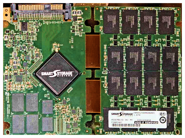
Tweaktown.com attended last week’s Flash Memory Summit and has published some great photos of the internals of the 2.5-inch SMART Storage 1.6Tbyte Optimus SSD. The drive has dual SAS ports with accompanying specs of 1Gbps sequential read and 500MGbps sequential write speeds using consumer-grade MLC (multi-level cell) NAND Flash memory.

An image of the guts of the drive (opened like a butterflied fish fillet) reveal two important facts. First, SMART Storage has designed its own SSD controller, putting it in good company with several other SSD vendors that have also decided to design their own controllers including Skyera, which I wrote about last week. The SMART Storage SSD controller is based on what the company calls the “Guardian Technology Platform,” consisting of:

  • FlashGuard, a technology that applies Flash-management and signal-processing techniques to improve the endurance of MLC NAND Flash.
  • DataGuard, which adds error correction to the SSD’s internal data paths.
  • EverGuard, a power-loss protection mechanism using capacitive energy storage.

Second, you can see from the image that the drive requires a 2-board assembly to hold 1.6Tbytes of Flash memory. The two boards appear to be joined with flex cables.

For more information about the Skyera Skyhawk announcement, see

Want to know Rado Danilak’s and Skyera’s plan for total enterprise-class SSD world domination?

How Skyera developed the 44Tbyte, enterprise-class Skyhawk SSD from the ground up. A System Realization story.

44Tbyte Skyera Skyhawk SSD employs Everspin MRAM as write cache

Posted in Flash, MLC, NAND, SAS, SSD, Storage | Tagged , , , , , , , , | Leave a comment

Memcon is filling up. Register now to be sure you get a ticket. It’s free. September 18. Silicon Valley

The Flash Memory Summit took place this week and registration for next month’s Memcon in Silicon Valley suddenly took a big uptick. I’d like to suggest that if you want to be certain to attend Memcon next month, you might want to register immediately. Like now. Registration is free.

The event takes place on September 18 at the Santa Clara Convention Center in the heart of Silicon Valley.

Parking is free.

Breakfast is free.

Lunch is free.

The knowledge is priceless.

Update: My gosh, how could I forget? Beer is free too.

Posted in DRAM, Flash, HMC, Hybrid Memory Cube | Tagged , , | Leave a comment

As seen at Flash Memory Summit: Whose car is this?

Leaving Flash Memory Summit on Tuesday, I stopped in my tracks when I saw this Toyota Corolla’s license plate. Can you decode it?

Posted in Flash | Tagged , , , | 1 Comment

Want to know Rado Danilak’s and Skyera’s plan for total enterprise-class SSD world domination?

This week, I reported on a new high-end, high-performance 44Tbyte SSD for data centers and server farms from Skyera. (See “44Tbyte Skyera Skyhawk SSD employs Everspin MRAM as write cache” and “How Skyera developed the 44Tbyte, enterprise-class Skyhawk SSD from the ground up. A System Realization story.”) Yesterday, Skyera’s CEO Rado Danilak gave a keynote speech at the Flash Memory Summit titled “Can Flash Be Mainstream Enterprise Storage – Now?” Of course, you know the answer to that question if it’s the title of a keynote speech at an event like the Flash Memory Summit. The answer, of course, is “yes,” Flash-based SSDs can be mainstream in enterprise storage, now. Danilak’s keynote essentially revealed his master plan for taking over the entire world of enterprise storage.

Who is this guy and where did Skyera come from? Rado Danilak was a founder and CTO of SandForce, the SSD controller IC vendor that’s now owned by LSI. These days, Danilak is Skyera’s CEO and his band of SSD experts is attacking a somewhat different problem—an enterprise-class problem. Here’s the problem statement in an easily digested slide from Danilak’s keynote presentation:

How can SSDs go mainstream in enterprise-class storage?

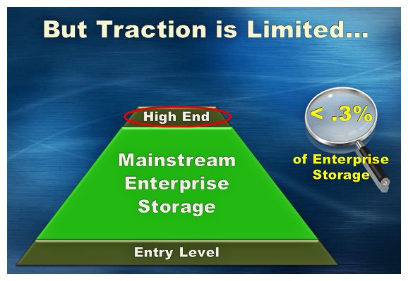
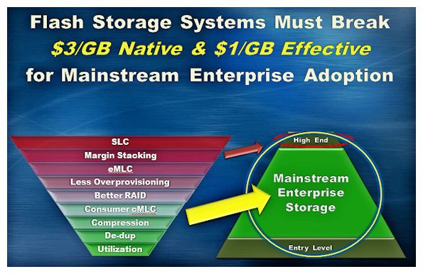
SSDs currently represent 0.3% of enterprise storage sales, taking only the topmost high-end position because of the cost per Gbyte for enterprise-class SSD storage. SSD performance is terrific relative to HDD storage but the SSDs’ cost is a barrier to widespread, mainstream enterprise adoption.

Here’s why:

Driving down the cost of enterprise-class SSD storage

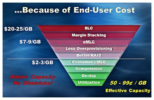
Build an enterprise-class SSD with SLC (single-level cell) NAND Flash memory to get good Flash endurance and system-level data reliability and you’ll charge $20 to $25 per Gbyte. There’s no mainstream goodness at that price point. So you need to drive the cost per Gbyte down if you want a mainstream storage product, down by about an order of magnitude according to Danilak. How? Well, you can use eMLC (enterprise multi-level cell) NAND Flash which delivers more capacity per dollar at the expense of some endurance. But that’s not going to get you all the way.

To get to the price levels Danilak thinks you’ll need to attain to go mainstream with an enterprise-class SSD product, you need to use commercial MLC NAND Flash memory. But that kind of NAND Flash memory cannot deliver enterprise-class endurance on its own. You need to add system-level magic including better Flash-specific RAID algorithms that can compensate for the loss of an entire NAND Flash device, better ECC algorithms, compression algorithms, and deduplication algorithms. Build a box that does all of this, and you can address mainstream enterprise-class storage needs.

That’s what this chart is supposed to show:

Lower costs per Gbyte will drive SSDs into mainstream enterprise-class storage

And that is what the Skyera Skyhawk SSD does.

Then what? Well, in a private conversation at the Flash Media Summit with Danilak and Alessandro Fin, Skyera’s VP of Product Management, I learned that the SSD controller in the Skyera Skyhawk is implemented in an FPGA to get the required performance from the RAID, ECC, and compression algorithms. This stuff can’t be implemented in software. Too slow.

The next logical step is to jump from FPGA to SoC. To do that, you need two things: a product that’s truly mainstream (to get the required sales volume) and a controller design that’s tested enough to be canned in silicon. Wanna bet on how soon that will be?

Posted in Flash, HDD, MLC, NAND, SSD, Storage | Tagged , , , , , , , | 1 Comment

How Wired’s Mat Mohan got his personal data back from his SSD after his MacBook Air was hacked. Hint: $1690 in recovery fees.

Mat Mohan knows how to transform adversity into opportunity. He’s a senior writer for Wired’s Gadget Lab and his Apple account was ingeniously hacked through a scam perpetrated on Amazon to get the necessary information to hack into Apple’s system. I read about his hacking adventure online and even heard him talk about it in a National Public Radio interview but that’s not the story here. In the process of being hacked, the SSD in Mohan’s MacBook was partially wiped and the rest of his data made inaccessible. He lost nearly 200Gbytes of personal data, photos, emails…the digital ephemera of 21st-century life.

Now, Mohan has written the story of how he got that life back. Essentially, he sent the partially erased drive to DriveSavers in Novato, California—a company that has specialized in retrieving digital data from damaged drives (hard and solid-state) for many, many years. It’s really a very interesting article that ends pretty well for Mohan even if the bill was $1690. He’ll make back more than the recovery cost when he publishes the book. Meanwhile, read the article here.

And do not miss DriveSavers’ “Museum of Bizarre Disk-asters.”

Posted in Flash, SSD, Storage | Tagged , , , , , , | Leave a comment

NVMe Emulator from Teledyne LeCroy emulates the SSD or the host controller

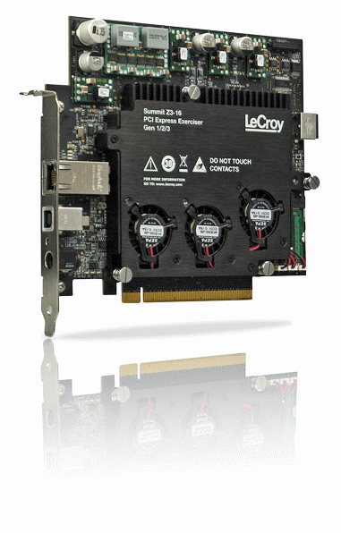
A PCIe-based emulator board from Teledyne LeCroy—the Summmit Z3-16 Exerciser—can emulate either an NVMe SSD or an NVMe controller, so it’s a good choice no matter what type of NVMe hardware you’re developing. It supports transfer rates of 2.5 to 8 GTransfers/sec and it has been chosen as the hardware test platform for the University of New Hampshire’s NVMe Compilance program managed by the UNH InterOperability Lab (UNH-IOL).

Posted in LeCroy, NVM Express, NVMe | Tagged , , , , | Leave a comment

Marvell’s DragonFly NVRAM and NVCACHE provide high SSD IOPS for large storage apps

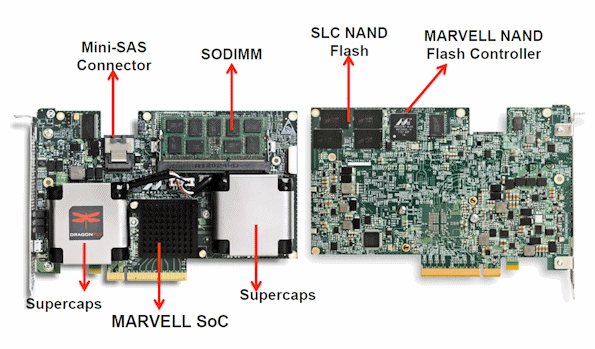
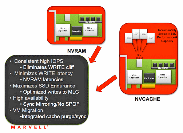
Marvell has just announced two new versions of its DragonFly PCIe board series: the DragonFly NVRAM and the DragonFly NVCACHE. Both boards contain a mixture of PCIe controller, SDRAM, SLC NAND Flash, supercapacitors, and software to create plug-in boards for expanding enterprise-class server storage capabilities.

Both boards interface to the server over a PCIe Gen 2, 8-lane implementation. The goal is to provide the server with consistently high IOPS capability through caching. The DragonFly NVCACHE board includes four SAS SSD interfaces and can control as many as four drives with a combined storage capacity of as much as 1.5 TBytes. The DragonFly NVRAM board is designed to work with external disk storage interfaces.

Using these new PCIe boards, server designers can achieve 4K random read/write performance of 220K IOPS with less than 22 microseconds of latency. The integrated ultracapacitors preserve the cached data long enough to back it up to the on-board NAND Flash memory in the event of a power loss, which is critical for enterprise-class servers.

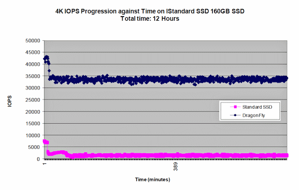
Here’s an IOPS graph showing you the difference in storage performance over an interval of hours with and without the Marvell DragonFly board.

Note: The SSD write cliff has already occurred before this plot starts so the blue and pink plots initially start at the same IOPS level somewhere to the left of this graph. Then the uncached SSD’s performance drops severely after the drive fills, initiating the write cliff, while the caching and drive-management software provided by the Marvell DragonFly board sustains a high IOPS performance level.

If you go to the Flash Memory Summit taking place in Silicon Valley this week, you should be able to see these boards in action at the Marvell booth.

Posted in Flash, Marvell, SAS, SSD, Storage | Tagged , , , , , , | Leave a comment

44Tbyte Skyera Skyhawk SSD employs Everspin MRAM as write cache

NAND Flash memory would be perfect for nonvolatile storage because except that Flash write speeds are slow enough to create a window of time when write transactions could be lost during a power failure. This problem is especially acute for enterprise-class storage. Skyera’s new 44Tbyte Skyhawk SSD storage system, being exhibited this week at the Flash Memory Summit in Silicon Valley, probably qualifies under the heading of “enterprise-class.”

44Tbyte Skyera Skyhawk SSD employs Everspin MRAM as a Write Cache

The Skyera storage system employs Everspin MRAM as a write cache for the system’s main storage medium, consisting of NAND Flash memory. The MRAM’s high write speed is the parameter that allows the MRAM to serve as the storage system’s write cache.

If nonvolatile MRAM were as inexpensive per bit as NAND Flash memory and if it were available in the kinds of bit densities as NAND Flash, there would be no need for the Flash devices at all. However, that’s not the case, so the NAND Flash memory serves as the medium for bulk storage and the MRAM is added in as a cache for the Flash.

If you’d like to hear more about this development, Everspin is presenting the idea in a talk titled “Enabling Write Cache with ST-MRAM” at the Flash Memory Summit on Wednesday, August 22.

Note: This is not the first time that the Denali Memory Report has discussed MRAM as a write cache for NAND Flash storage. See the May 30, 2012 blog post: “MRAM spotted in Buffalo Memory SSD—for cache.”

Update: For more in-depth technical details on the Skyera Skyhawk SSD, see “How Skyera developed the 44Tbyte, enterprise-class Skyhawk SSD from the ground up” in the EDA360 Insider.

Posted in Flash, MRAM, NAND, SSD, Storage | Tagged , , , , , , | 3 Comments

Seen on the street: WD needs SSD Engineers

Drinking coffee with my friend Ira Feldman on Friday at the Starbucks behind Cadence, this advertising truck pulled up and parked for a while. Must be some sort of sign about the growing popularity of SSDs. I wonder how many engineers they can fit in that truck? They’d better be skinny.

Posted in SSD | Tagged , , , | Leave a comment

Be sure to come back on August 21

There are several key announcements queued up on the Denali Memory Report, timed to coincide with the start of the Flash Memory Summit on Tuesday.

Posted in Uncategorized | Leave a comment

Friday Video: A personal invitation to Memcon from Sanjay Srivastava

Want to know why you need to be at Memcon this year? Here’s Denali Software founder Sanjay Srivastava to tell you why:

Now go and sign up! It’s a free ticket and includes breakfast, lunch, and some goodies—not to mention the great information you’ll hear. Register by clicking here. Now.

Posted in DDR3, DDR4, DRAM, Flash, HMC, Hybrid Memory Cube, JEDEC, LPDDR2, LPDDR3, LPDDR4, Memcon, MRAM, mSATA, NAND, NOR, NVM Express, NVMe, ONFI, PCIe, Samsung, SAS, SATA, SD, SDRAM | Tagged , , , | Leave a comment

IDT to present on NVMe at next week’s Flash Memory Summit in Silicon Valley

Flash Memory Summit is next week in Silicon Valley and IDT is giving a presentation on the NVMe standard for PCIe-based SSDs. Peter Onufryk, director of engineering in the Enterprise Computing Division at IDT, will present “How the Streamlined Architecture of NVM Express Enables High Performance PCIe SSDs.” The presentation will provide an overview of NVM Express along with a detailed outline of the specification’s performance features.

Today is the last day to register for the Flash Memory Summit online and it’s the last day to get a free exhibits-only pass to the event. Click here to register.

Posted in NVM Express, NVMe | Tagged , , , , , , | Leave a comment

Can you make money selling DRAM? The Memory Guy says “yes,” but perhaps not all of the time

Jim Handy, The Memory Guy, has decided to become a Mythbuster with respect to the meme: “You cannot make a profit in the DRAM manufacturing business.” He just published a blog post titled “Is DRAM Really a Profitless Business?” This blog post contains a plot that shows aggregate profits for the DRAM industry from 1991 through 2011. Cutting to the chase, the industry’s aggregate revenue for this time period was $477 billion. Average profit over 21 years: $200 billion.

How does Handy know? He’s “The Memory Guy.” It’s his business to know.

Here’s a thumbnail of Handy’s/Memory Guy’s chart:

To see the real thing, go read The Memory Guy’s blog post.

Posted in DRAM | Tagged , , , | Leave a comment

Flash memory endurance, multi-level cells, and process technology

I’ve been following an interesting discussion about Flash memory endurance, multi-level cells, and process technology in the LinkedIn Solid State Storage Group. Yesterday, The Memory Guy Jim Handy stepped in with this comment:

“Flash endurance is the result of disruptions in the tunnel oxide layer. The disruptions come from the stress the high programming fields induce during programming. When enough of these disruptions occur they link together into a short circuit that prevents the floating gate from maintaining a charge.

…The phenomenon that gives MLC worse endurance than SLC is the spreading of the voltage distributions of the multilevel bits as the tunnel oxide disruptions start to trap charges.

What is interesting, though, is that only one bit fails at a time, so a block with eight bit errors must be decommissioned if 8-bit error correction is being used, but this same block performs just fine with higher levels of error correction. 48-bit error correction like that used by Link_A_Media will clearly get very good block endurance out of MLC or even TLC flash.

Really sophisticated controllers use other techniques to manage behavior internal to the flash chip itself, sometimes even changing voltage thresholds and programming algorithms to coax even more life out of each cell.

…The endurance of the flash decreases as the number of bits per cell increases, and it also decreases as the process technology shrinks, forcing controller makers to keep improving their error correction and flash management techniques.”

You might want to take a look at the whole discussion, if you’re a member of LinkedIn.

Posted in Flash, NAND | Tagged , , , , , | Leave a comment

Initial Hybrid Memory Cube short-reach interconnect specification issued to Consortium adopters

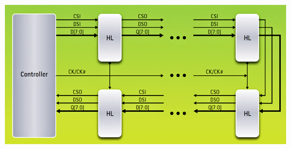
The Hybrid Memory Cube Consortium (HMCC), now supported by the three top DRAM vendors (Samsung, SK hynix, and Micron), has just issued an initial draft specification for the Hybrid Memory Cube’s “short-reach interconnection across physical layers”—in other words, the short-reach PHY—to adopting members of the Consortium. As the Hybrid Memory Cube has evolved, it’s become apparent that two PHY specifications would be needed: a short-reach spec for interconnections on FR4 circuit boards with trace lengths to perhaps 10 inches and a low-power “ultra short-reach” spec for interconnections in multichip modules and in 2.5D assemblies with trace lengths of perhaps 2-3 inches. The energy consumption for the short-reach PHYs is expected to be on the order of 5-10 pJ/bit and the energy for the short-range PHY is expected to be “much less” than 5pj/bit, according to Micron Technology Strategist Mike Black.

The initial target application focus for the Hybrid Memory Cube includes high-performance networking, industrial equipment, and test and measurement. Although these applications share many memory-specific requirements, they do have differing needs that are accommodated through settings in a mode register within the Hybrid Memory Cube. Details are still confidential but an example of an application-specific mode setting might be the serialized packet size used to communicate between the Hybrid Memory Cube and the host system.

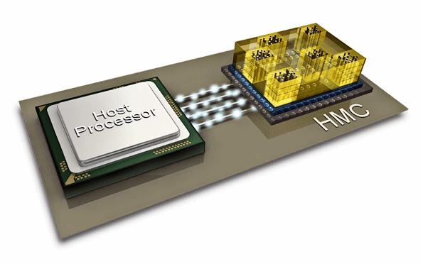
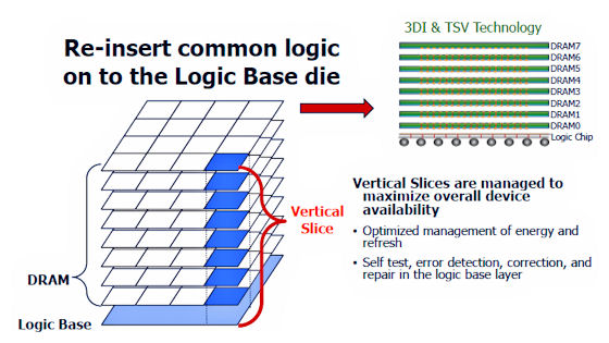
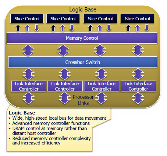
If you’re not familiar with the Hybrid Memory Cube, it’s a development initiated by Micron to extract much more of the inherent data parallelism in today’s DRAMs, which are all based on multiple on-chip DRAM arrays. Conventional DRAM design funnels the I/Os from all of the on-chip arrays through one memory interface—a real bottleneck. Through 3D assembly, the Hybrid Memory Cube gives each of 16 on-chip memory arrays a clear path to a base logic chip where there are memory controllers and SerDes interfaces for high-bandwidth connection to the host system.

Here’s an illustration of what a Hybrid Memory Cube might look like:

For more information about the Hybrid Memory Cube, see:

Posted in 3D, DRAM, HMC, Hybrid Memory Cube, Hynix, Micron, Samsung | Tagged , , , , , , | Leave a comment

Plextor blog walks you through the design process for the PX-M5S SSD: better, faster, cheaper

Plextor has just published an extremely interesting blog post that walks you through some of the high-level design decisions behind the company’s new PX-M5S SSD. According to the design goals, the prioritized objectives are:

1) speed
2) reliability
3) price

Then the blog post draws a line in the sand (silicon?):

“Plextor SSDs generally cost more than competing SandForce-based SSDs since they use a more expensive server-grade controller from Marvell, exclusive firmware, high quality flash memory from Toshiba, and surface mount components built by Japanese firms that settle for nothing less than obsessive tolerances.”

And finally, the blog post notes what’s different about the design of the PX-M5S SSD:

“The Plextor PX-M5S uses a different NAND supplier, and is priced more competitively than the previous M3 Series of SSDs, while still upping the bar in performance. For the M5S, Plextor turned to Micron to supply 25nm synchronous NAND flash, a product of equal quality to Toshiba Toggle NAND, but more available than the 24nm Toshiba Toggle Mode flash used on the M3S and M3 Pro.”

It’s extremely unusual for an SSD vendor to provide this level of insight into one of its designs yet the Plextor post continues in even more detail:

“Toggle technology is primarily used [manufactured] by Toshiba and Samsung, and carries data at a speed of 133MBytes/sec. In the ONFI (Open NAND Flash Interface) camp, the key manufacturers are Intel, Micron and Hynix… ONFI 1.0 (or Asynchronous NAND) is limited to a 50MBytes/sec transfer rate, but ONFI 2.0 (called Synchronous NAND) has a transfer rate of 133MBytes/sec. The key difference between ONFI 1.0 (Async) and ONFI 2.0 (Sync) NAND is its interface speed and, remember, speed counts with SSD users.”

Some of the specs for the SSD are pretty impressive including a sequential read speed of 520 Mbytes/sec and a sequential write speed of 200 Mbytes/sec. A 128GByte PX-M5S SSD lists at $149.99 on the Plextor site.

Posted in NAND, ONFI, SSD, Toggle | Tagged , , , , , , | Leave a comment

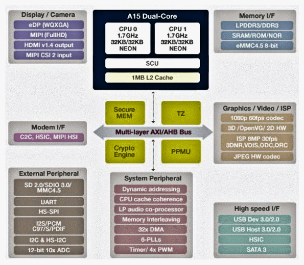
Samsung Exynos 5 Dual mobile processor features two 1.7GHz ARM Cortex-A15 processors, a WQXGA display controller, and two LPDDR3 controllers to feed ‘em

The Web was abuzz this weekend with the unveiling last week of the Samsung Exynos 5 Dual mobile processor, which features two 1.7GHz ARM Cortex-A15 processors. The previous generation of Exynos Dual mobile processor incorporated two 1.4GHz ARM Cortex-A9 processor cores. Between the ARM Cortex-A15 processor’s additional clock rate and its improved instructions/clock figure of merit (1.5x better for integer processing and 2x better for floating-point processing), Samsung says that the Exynos 5 Dual mobile processor has twice the processing bandwidth of the previous generation.

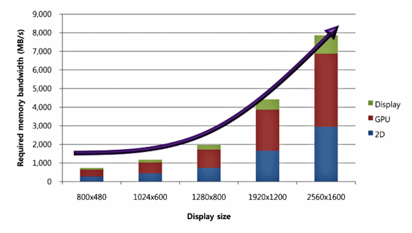
However, these two leading-edge CPU cores are not the only significant feature of this new mobile processor chip. It also includes a controller for 2560×2048-pixel WQXGA displays (also known as the “Wide Quad Extended Graphics Array”). Worst case, a WQXDA display controller operating at 60 frames/sec and 24 bits/pixel requires 8 Gbytes/sec of memory bandwidth. However, that’s with the display controller getting the entire memory interface. As the Samsung Exynos 5 Dual White Paper points out, assuming the display controller “only” takes 80% of the memory bandwidth, the chip will need 10 Gbytes/sec of memory bandwidth and that’s giving the two ARM Cortex-A15 processors a mere 2 Gbytes/sec  of memory bandwidth to share.

Here’s a graph of display resolution versus memory bandwidth from the Samsung Exynos 5 Dual White Paper.

Consequently, the designers of the Exynos 5 Dual mobile processor added two 800MHz LPDDR3 memory controllers to the design. Together, these SDRAM controllers can generate a peak bandwidth of 12.8 Gbytes/sec of memory traffic between the Exynos 5 Dual mobile processor and the attached LPDDR3 1600 SDRAMs.

Here’s a block diagram of the Exynos 5 Dual mobile processor:

For more in-depth information on the ARM Cortex-A15 processor core, see:

Want some Top Secret ARM Cortex-A15 implementation info?

Would you like some ARM Cortex-A15 resources to peruse?

The WORD on ARM’s big.LITTLE Cortex-A15/A7 design philosophy from Jack Ganssle, a leading expert and consultant on embedded design and firmware development

Realizing the ARM Cortex-A15: What does the road to 2.5GHz look like?

Want to know the secrets of implementing an ARM Cortex-A15 in an advanced process node? Read on!

ARM Cortex-A15—does this processor IP core need a new category…Superstar IP?

To get your own copy of the Samsung Exynos 5 technical White Paper, click here.

Posted in ARM, Cortex-A15, Exynos, LPDDR3, Samsung | Tagged , , , , | Leave a comment

Beware of Geeks bearing gifts (SSDs)?

I love this article in Bloomberg Businessweek titled “Samsung Sends Out Geeks to Revamp Laptops With New Drives.” It reports that Samsung placed a roving pan-European army of “geeks” in the UK, France, and Germany to ambush pedestrians and offer to perform an SSD transplant on their laptops—on the spot. What a great publicity stunt: drive-by upgrades. Apparently 42 people accepted gifts from the geeks.

Posted in Samsung, SSD | Tagged , , , , , | Leave a comment

Are Enterprise SSDs a “bad” idea? Four tips and counter-tips for your consideration.

I ran across a commentary on the Kaminerio Web site, “Is SSD Really a Bad Idea? BE CAREFUL WHOSE ADVICE YOU TAKE” by Eyal Markovich, which is a reaction to a blog posting by Phil Goodwin on the SearchSolidStateStorage.com Web site titled “When using SSD is a bad idea.” (Sorry, the SearchSolidStateStorage.com site requires free registration.) Markivich’s reaction was not to argue but to provide some really valuable commentary on the SearchSolidStateStorage.com tips for using SSDs.

These tips and the Markovich responses bear posting here at the Denali Memory Report in shortened form:

Tip1: Don’t Use an SSD when applications are not read intensive.

Markovich’s response: Memory cell wear is really a function of average write IOPS, not simply whether an application is write heavy or not.

Tip 2: Don’t Use an SSD when data access is highly random.

Markovich’s response: Whether data access is random or sequential, an SSD will give you much better performance than a hard disk.

Tip 3: Don’t use general-purpose SSDs in highly virtualized environments.

Markovich’s response: An enterprise SSD storage solution, such as a K2 that scales to 100TB, makes a fabulous solution for improving the performance of virtual environments.

Tip 4: Don’t Deploy Consumer Grade SSD for enterprise applications.

Enterprise SSD solution vendors employ a raft of techniques and technologies to greatly extend the life of MLC, giving you long SSD life at a much lower cost than SLC or even eMLC.

…for your consideration.

Posted in SSD, Storage | Tagged , , , , , | 1 Comment

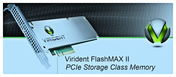
Virident Systems introduces PCIe SSD with capacities to 2.2Tbytes, high IOPS

Virident Systems has announced the Virident FlashMAX II, the company’s next-generation PCIe SSD for enterprise environments. According to the company, the FlashMAX II features the highest capacity (550Gbytes to 2.2Tbytes) in a low-profile PCIe plug-in card format, with industry-leading performance (48,000 to 350,000 Read IOPS and 105,000 to 217,000 Write IOPS). The FlashMax II also features support for VMware ESXi and VDI environments for optimal performance of virtualized desktops and applications. Pricing for the FlashMAX II PCIe SSD starts at $6000.

PCIe SSDs deliver appreciably more IOPS performance than SAS and SATA SSDs. For more on PCIe SSds, see the Denali Memory Report’s coverage of a previous announcement of a PCIe SSD from this same company, “Virident PCIe SSD delivers 320,000 read IOPS with 24-year service life.”

Posted in PCIe, SSD | Tagged , , , , , | Leave a comment

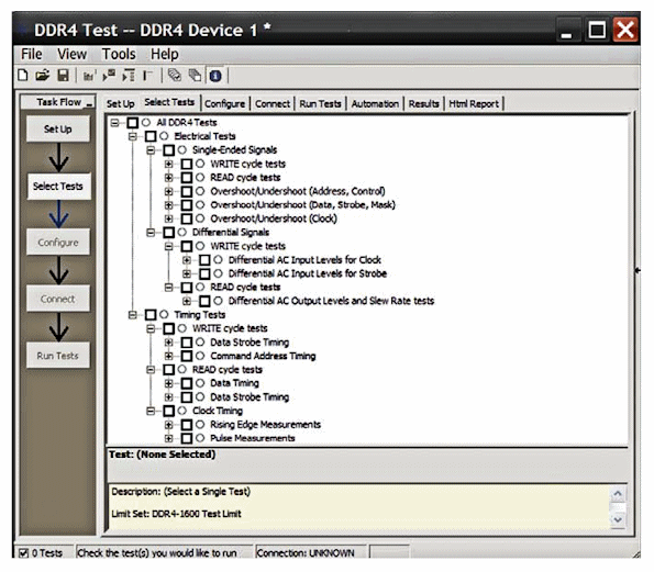
Test your system design for DDR4 JEDEC compliance with this $4500 ‘Scope add-on

Agilent has just announced a compliance test application for DDR4 SDRAM system designs. The $4500 Agilent N6462A DDR4 test application accelerates bring-up and debugging of DDR4 SDRAM-based systems by automating a bevy of physical-layer I/O testing with the company’s 9000 and 90000A, 90000 X-Series, and 90000 Q-Series oscilloscopes. The automated test roster includes compliance testing of clock jitter, electrical, and timing measurements in accordance to the JEDEC DDR4 SDRAM specifications from DDR4-1600 through DDR4-3200 speed grades. Automated tests include:

  • Single-ended and differential electrical parametric tests
  • Read and Write tests
  • Timing tests
  • Clock-timing tests

Note: Agilent will be exhibiting at Memcon next month. For registration details, click on the banner over there to the right of this blog post.

Posted in DDR, DDR4, DRAM, SDRAM | Tagged , , , , , | Leave a comment

How many SSDs does it take to saturate PCIe Gen 3? Would you believe 16 drives?

It’s now possible to conduct some interesting performance tests on real PCIe Gen 3 products and the video below shows you a PCIe Gen 3 RAID card talking to 16 SSDs, which is the number of drives needed to saturate a setup based on an Intel Sandy Bridge processor and chip set. The result is 6600 Mbytes/sec of throughput—about 90% of the theoretical maximum [for an 8-lane implementation of the PCIe Gen 3 protocol]. With tweaking, that number might go up to 95%. Just watch the video.

For information on the PCIe Gen 3 IP used in the creation of the Adaptec RAID SoC, click here.

If you’d like to see this demo LIVE, sign up for this month’s Flash Memory Summit, but hurry, the online discount’s going away soon.

Posted in PCIe, SSD, Storage | Tagged , , , , , , | 3 Comments

Save the date: JEDEC DDR4 Workshop, Santa Clara, CA. October 30-31

JEDEC is sponsoring a 2-day DDR4 workshop that should interest anyone planning on using DDR4 SDRAM in next-generation designs.

Day 1:

  • DDR4 vs DDR3: Comparison Matrix
  • Why migrate to DDR4
  • Power-on, initialization, and training
  • Read/Write and refresh operation review

Day 2:

  • Manufacturability and reliability issues
  • DDR4 power-saving features, modes, and techniques
  • DDR4 3D arrays
  • DDR4 module outlook

The event takes place on October 30-31 at the Santa Clara Marriott in the center of Silicon Valley. Click here for more details.

Posted in DDR4, DRAM, SDRAM | Tagged , | Leave a comment

Fast update on STT MRAM vendor Avalanche Technology: They’ve been here since 2006

Alan Niebel, CEO of Web-Feet Research, commented via LinkedIn on yesterday’s blog post about STT MRAM vendor Avalanche Technology:

“Avalanche has been in the STT MRAM race for over four years now. They are not late to the party, they are some of the party leaders.”

My apologies to Avalanche. The post itself was a straightforward discussion of the company’s 3rd-round financing announcement. The headline could be interpreted as suggesting that Avalanche was new to the STT MRAM arena; it certainly wasn’t meant to suggest that Avalanche was late to the STT MRAM party. According to the company’s Web site, Avalanche was founded in 2006 and announced an $11.5 million 2nd funding round in January, 2012.

The most recent press release says that the 3rd funding round will allow the company to go into production with its STT MRAM product. I am not aware of any company presently in production with an STT MRAM product, so no one’s late to the party.

Posted in MRAM | Tagged , | Leave a comment

Flash Memory Summit: Great Program on Non-Volatile memory.

The Flash Memory Summit rolls into Silicon Valley – August 21-23. Here’s a summary of topics covered in the program:

  • Flash Memory-Based Architectures
  • Next-Generation Flash and SSD Controllers
  • Solid-State Drive (SSD) Technology
  • Enterprise SSDs
  • Testing/Performance/Endurance
  • NVMe
  • LDPC Coding
  • Enterprise Storage Applications
  • Flash and Virtualization
  • Flash in Data Centers
  • Enterprise Caching
  • Client Caching

In addition, there’s an IEEE Milestone plenary tells how the technology started 25 years ago.

If you’re at all associated with or interested in Flash, you will want to attend. Online pricing ends on August 16, by the way.

Click here for more information.

Click here to register.

Posted in Flash, mSATA, NAND, NOR, NVM Express, NVMe, SSD, Storage, Toggle | Tagged , , , | Leave a comment

Add Avalanche Technology to the growing list of vendors in pursuit of STT MRAM

EEtimes reports http://www.eetimes.com/electronics-news/4391539/Startup-raises-money-to-bring-MRAM-to-market?pageNumber=0 that Avalance Technology http://www.avalanche-technology.com/ has just gotten $30 million in funding from Avalanche’s current investors (Vulcan Capital, Sequoia Capital, Bessemer Venture Partners, Thomvest Ventures and Qualcomm Ventures) and VTB Capital (Moscow, Russia). The investment is to help Avalanche ready its spin-torque-transfer (STT) magnetic RAM (MRAM) for production. Avalanche is one of a number of companies that are questing for commercial STT MRAM, hoping to displace some or all of the NAND Flash market.

For much more information about MRAM and MRAM vendors, register for Memcon over there on the right. Also, see:

Posted in Uncategorized | Leave a comment

See the future of DRAM usage, at least until 2015. Marc Greenberg from Cadence lays it out in a video

This year at DAC, Marc Greenberg gave a presentation on the near- and medium-term future of DRAM in the ChipEstimate booth. Two separate technology paths will dominate: the PC/server space and the mobile space. By 2015, PCs and servers will be using three (or more) channels of DDR3 or DDR4 SDRAM and mobile devices will have migrated to LPDDR2, LPDDR3, and Wide I/O formats.

Processors in both of these spaces will actually consist of multiple heterogeneous and homogeneous processing elements all vying for SDRAM access, a situation that places many demands on the SDRAM controller. For example, just by reordering traffic to the SDRAM(s), the DRAM controller can improve memory bandwidth by 30%. At the same time, these newer SDRAMs have low-power modes that can be used to advantage by the controller.

For these insights and more, watch the video:

Posted in DDR, DDR3, DDR4, DRAM, LPDDR2, LPDDR3, Wide I/O | Tagged , , , | Leave a comment

You say “memristor” and I say…something else? Amusing comments from the memristor naming debate.

You may or may not be aware of a small controversy surrounding the use of the term “memristor” by HP’s Stan Williams (See “Wonks Question HP’s Claim to Computer-Memory Missing Link” at Wired.com) I’m not going to weigh in on that argument, the device does something useful that can clearly be used as a non-volatile memory no matter what you name it. However, I got a real kick out of some Slashdot comments and wanted to share them:

“I feel like I’m eavesdropping in the middle of a conversation between two mental patients.”

“Personally, I still have no idea.”

“So, what gives if this HP invention is not the ‘perfect’ memristor. As long as it’s close enough, it would do. In other words: if it quacks like a duck…”

“I came here to say precisely this. It isn’t an ‘ideal’ component. Which is what the theory is based on. But then neither is any electrical component you can think of. Even resistors stop being linear at very high or very low voltages / currents. Anybody ever seen an ideal current source? An ideal voltage source? And ideal op-amp? Its not ideal because it is a real device. Ideal components only exist on paper.”

“What HP have produced is a device that substantially behaves like a memristor, if you are only measuring current and voltage at the terminals. That’s useful if you want to build a memory device, since the behaviour is such that resistance will vary with the integral of the current through it.”

“Terminology IS important. Suppose HP gets a patent on their “memristor”, and suppose someone else discovers a true memristor within 20 years. The HP “memristor” could set back the state of science with stupid patent lawsuits for a generation.”

“Do any of the previous posters have any actual experience dealing with memristors? My phone rang off the hook when this BS story hit the Internet a few years ago. I worked at QuckLogic, where we built “memristors”, but failed to have the marketing brilliance to call them anything other than “antifuses”. I don’t blame the guy at HP who did pull this off. That’s how the game is played.”

Note: You’ll find these comments at http://hardware.slashdot.org/story/12/07/25/2127229/the-hp-memristor-debate?utm_source=feedburner&utm_medium=feed&utm_campaign=Feed%3A+Slashdot%2Fslashdot+%28Slashdot%29

Posted in Memristor | Tagged , , , , , | Leave a comment

Unigen (and others) continue to roll out new mSATA SSDs

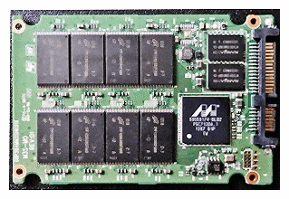
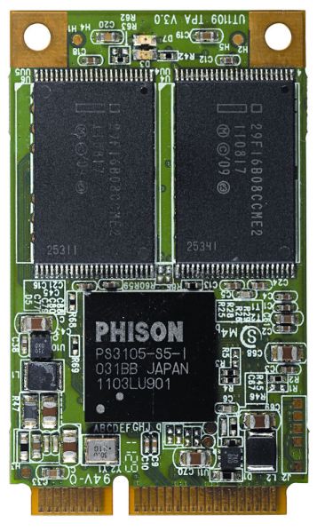
The Mini-SATA or mSATA form factor and interface standard for SSDs has been around since September, 2009 and it now seems to be gaining substantial traction in the form of several new product introductions over the last couple of months. The product introduction that triggered this blog entry is the announcement this month by Unigen that rolled out three mSATA SSDs: Models 2202 and 2204 for applications that require high-performance random access and the Model 2512 that is more targeted to applications involving “incompressible” data such as the storage of pre-compressed video, image, and audio files. All drives employ a SATA III interface that operates at 6Gbits/sec and ship next month.

Here’s a photo of a Unigen mSATA drive:

Many comments to be found in online credit Lenovo for helping to make the mSATA form factor suddenly popular. For example, here’s one such credit from thessdreview.com site:

“For the most part, we have Lenovo to thank for that as millions of Thinkpad owners played a key role in mSATA SSDs flying off the shelves quicker than they could restock.   Industry has responded well, however, as mSATA becomes the new ‘SSD Du Jours’ for the new ultra crowd.”

Other mSATA drives announced within the last month or two include:

Posted in mSATA, SSD, Storage | Tagged , , , , , , | Leave a comment

Want the latest scoop on DDR4 DRAM? Here are some technical answers from the Micron team of interest to IC, system, and pcb designers

DDR4 SDRAM is on the way. Just his month, Samsung announced sampling of its 16Gbyte DDR4 SDRAM RDIMMs (registered DIMMs) based on its 30nm-class DDR4 SDRAM chips. Production is slated for next year. Micron has announced plans for volume DDR4 SDRAM production even earlier, late this year. The design of SoCs and other sorts of devices with integrated DDR4 memory controllers is already well underway. I recently gave some questions about DDR4 SDRAM to the memory guru at Cadence, Marc Greenberg and he sent the questions along to Micron. Andreas Schlapka, Senior Product Line Manager at Micron Technology, and his team at Micron supplied these interesting answers:

Why did we need a DDR4 spec? Couldn’t we extend DDR3?

[The need for] increasing memory speed has been a challenge to the DRAM industry for decades. Rising energy costs and the focus of mobile power consumption make memory power and energy consumption important factors as well. DDR3 has been extended beyond its initial capabilities by adding higher data rates (1866 and 2133 Mbytes/sec) and reducing the [supply] voltage (from 1.5V to 1.35V). DDR4 is now enabling the industry to go well beyond the extension of DDR3—with data rates to 3200Mbytes/sec and an operating voltage of only 1.2V.

What three things do IC designers most need to know about DDR4 to build first-time-right SoCs that can control DDR4 SDRAM?

The top three topics the designers need to take into account for with DDR4 memory are:

  1. VrefDQ Calibration, new addressing schemes and the power saving features.  DDR4 requires that the VrefDQ calibration be performed by the controller.
  2. There are several new address schemes which include bank grouping to maximize effective bandwidth, ACT_n activate pin to replace RAS#, CAS#, and WE# commands, PAR and Alert_n for error checking and DBI_n for data bus inversion.
  3. There are a multitude of new [DDR4] power-saving features including Low Power Auto Self Refresh, Temperature Controlled Refresh, Fine Granularity Refresh, Data Bus Inversion, and CMD/ADDT latency.

What three things do board-level designers need to know about DDR4 that they didn’t need to know with DDR3?

The first topic that board-level designers need to account for is the new power supplies, VDD/VDDQ = 1.2V and VPP = 2.5V (wordline boost). The next difference is that VrefDQ is supplied by the DRAM internally while VrefCA is supplied by the board. And lastly, DQ pins are terminated high via pseudo open drain I/O unlike the CA pins that are center-tapped to VTT (like DDR3).

How far will DDR4 take us and for how long?

The final details of the DDR4 standard especially on the module definition are soon to be closed in JEDEC. Major DRAM suppliers have first samples available and [design] work at enablers and OEMs is ongoing to ramp up the first systems in early 2013. The volume cross over between DDR3 and DDR4 is expected in 2015. Based on the historical lifetime for a DRAM technology of about 4 years, any DDR4 successor would need to become available 2017, with volume cross over in 2019. But so far it’s unclear what this new technology could look like. Once the standardization work on DDR4 is done, the industry will focus on next steps and evaluate concepts like HMC (the Hybrid Memory Cube) for the next-generation mainstream DRAM.

For more information on DDR4 SDRAM, see these earlier blog posts:

The DDR4 SDRAM spec and SoC design. What do we know now?

Samsung starts to sample 16Gbyte DDR4 LRDIMMs using 30nm-class DDR4 memory chips

Micron samples DDR4 module at 2400Mtransfers/sec. Production pegged in 2013

Memory to processors: “Without me, you’re nothing.” DDR4 is on the way.

JEDEC releases more details about DDR4 SDRAM spec. Want to know what they are?

Posted in Uncategorized | Leave a comment

How many DRAMs does it take to populate a supercomputer? 746,496 plus a lot of hot water for cooling

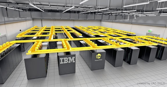
Jim Handy, The Memory Guy, posted a short blog about the 3-petaFLOP (peak) SuperMUC supercomputer at the Leibniz Supercomputing Centre on the outskirts of Munich, Germany. (The “MUC” in SuperMUC is the 3-letter code for the Munich airport. Now that’s esoteric!) Based on the Samsung announcement, the SuperMUC’s 147,456 microprocessor cores contained in 18,432 Intel Xeon Sandy Bridge-EP multicore microprocessors are teamed with 324Tbytes of Samsung Green 30nm-class DDR3 SDRAM modules. By Handy’s calculation, that’s a total of 746,496 DRAM chips.

Sounds like a lot, no? Well, Handy’s calculations say that’s about half a day of fab production for one of Samsung’s DRAM fabs. Using an average market price of $10.45 per Gbyte for the past year, Handy then calculates that the value of the DRAMs is perhaps as much as $3.5 million, although with the volume purchase we’re talking about here, it’s likely less.

But the absolute cost of the DRAM is not the point.

The point is that the SuperMUC requires “only” 3.52 MWatts of electricity to run, which Handy pegs at $3 million per year, not including cooling costs. When you include cooling costs, one year’s worth of electricity to power and cool the SuperMUC costs more than the DRAM.

But wait, there’s more.

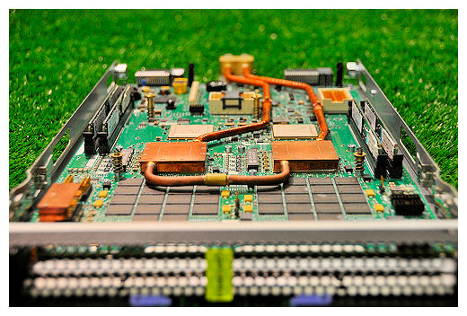
The SuperMUC uses an unusual hot-water cooling system to cool the Xeon processors. It’s a new form of cooling invented by IBM (the system supplier of the SuperMUC) called Aquasar, which reportedly cuts the energy needed for cooling by 40% by using 60°C (or perhaps 45°C depending on the reference) water for cooling. The cooling water is piped through copper cooling blocks directly connected to the processor die. The water flows through microchannels in the copper. Here’s a photo of an Aquasar processor module from Wikipedia:

More Aquasar details here.

You don’t need as much energy to chill water down to 60°C as you do to make it colder. During winter months, waste heat from the SuperMUC will be used to heat buildings.

Posted in DDR3, DRAM, Samsung, SDRAM | Tagged , , , , , , , | 1 Comment

Who do you want to see at Memcon?

As the emcee for the Memcon event on September 18, I’ve been given the opportunity to personally invite a few, select exhibitors to the show and to cut them a very sweet deal. To do that, I’d like to know who you would like to see as an exhibitor at Memcon this year. Your favorite Flash or DRAM vendors? (Who?) Your favorite MRAM or Memristor vendors? Your favorite SSD or memory module vendors? Just leave me a comment on this blog or, if you’re connected to me via LinkedIn, send me a message. Or, if you already have my email address, fire off an email to me.

I’ll do my best to get them to the show so you can talk to ‘em.

Oh, and if you haven’t signed up yet, click on that Memcon banner—over there on the right. It’s an event you probably won’t want to miss.

Thanks,

–Steve Leibson

Posted in DDR, DRAM, Flash, MRAM, NAND, SSD | Tagged , , , , , , , | Leave a comment

Cool case instantly transforms 2.5-inch HDD or SSD into WiFi-connected network storage

Patriot Memory is now selling the Gauntlet Node, a cool name for a cool disk-drive case that transforms a 2.5-inch HDD or SSD into a WiFi-connected network storage device. The enclosure has an internal SATA port and can accommodate drive capacities to 2Tbytes. There’s also an external USB port.

Transfer rate over the WPA-secured WiFi a/b/g/n link is 150Mbits/sec. There’s an internal battery that will power the drive for as long as five hours of continuous streaming and an external dc power port for always-on operation. In addition, Patriot Memory has iOS and Android apps for connecting devices to the storage device.

The price? $99.99, drive not included.

Posted in HDD, SATA, SSD, Storage | Tagged , , , , , , | Leave a comment

Want more details about the new Micron 1Gbit Phase-Change Memory / 512Mbit SDRAM device? Here are several

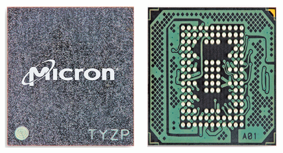
Yesterday, Micron announced volume production of a new memory device containing one 1Gbit PCM (phase-change memory) die and one 512Mbit LPDDR2 SDRAM die. This morning, I had a conversation about this new device with Philippe Berge—Senior Director of the NOR, PCM, e.MMC Business, Wireless Solutions Group at Micron Technology—who gave me some additional technical details.

The first question I asked was about whether or not the device had a part number, which is simply an easier linguistic handle to use when writing about the memory component. Because the device is targeted at the high-end of the feature phone market and is not a catalog part, it doesn’t have a part number that Micron cares to publicize. So I’ll continue to refer to it as “the device” in this blog.

Berge said that this announcement of a 1Gbit PCM/512Mbit SDRAM combo device is the first of many such high-volume devices aimed at feature phones and other mobile devices. The end-product targets for this device and others in the family are the sockets for NOR Flash memory and SDRAM in feature-phone handsets. The device that Micron announced yesterday is for high-end feature phones. According to Berge, smaller-capacity devices in the family will follow and Micron will start to discuss the use of these devices in other markets next year.

The technical specs for the newly announced memory device are fairly interesting. The PCM die and the SDRAM die share an LPDDR2 interface. That means that the PCM die employs the LPDDR2-NVM interface protocol. The two die reside in the device package as stacked die, with wire-bonded interconnect. This is a common form of 3D IC assembly that’s long been in use for mobile phone handset components to reduce component footprint and therefore printed-circuit board area. In this case, the design also reduces end-product manufacturing cost because the application processor needs only one interface and possibly only one memory controller to communicate with the PCM device and the SDRAM. There are also fewer printed-circuit traces to deal with using this approach.

The device’s LPDDR2-NVM interface employs 400MHz, double-data rate transfers so the supported memory bandwidth is fairly high. One important end-product characteristic aided by this high bandwidth is boot time. It simply takes less time to get the boot code out of the PCM compared to NOR Flash memory.

PCM brings two additional performance enhancers to the party. The first is the elimination of the erase cycles required by NOR Flash memory when writing to the non-volatile memory. PCM is bit-alterable without the need for an erase cycle. This attribute speeds write times and simplifies the associated software.

The second performance enhancer is the PCM’s write speed, which is 10Mbytes/sec in this new Micron device. NOR Flash typically supports write speeds of less than 1Mbyte/sec. That’s at least a 10x difference, depending on the NOR Flash device used for comparison.

Finally, I’ve written in the past about a possible problem with PCM self-erasure due to ambient temperature. The new Micron device’s temperature rating is -25 to +85°C. Self erasure is not an issue for this device, according to Berge.

For the previous blog entry about the Micron announcement, see “Micron announces volume production of PCM/DRAM multichip packaged memory”.

For more information on the LPDDR2 and LPDDR2-NVM interfaces, see “LPDDR2: The new mainstream memory for embedded and mobile applications?

For additional information on previous PCM announcements, see “Numonyx 128-Mbit serial- and parallel-I/O PCM non-volatile memories now available in volume,” and “Samsung announces imminent release of a multichip module integrating DRAM and PCM for Smartphone applications

Posted in DDR, Flash, LPDDR2, Micron, NOR, PCM, Storage | Tagged , , , , , , , | Leave a comment

Micron announces volume production of PCM/DRAM multichip packaged memory

Totally not expecting this. Today Micron announced high-volume availability of a multichip, packaged memory device that incorporates a 1Gbit PCM (Phase-Change Memory) and a 512Mbit LPDDR2 SDRAM. The PCM die is built with 45nm process technology. The multichip-packaged memory is aimed at mobile devices because of the low-power, high-performance, and small footprint of the combined PCM/SDRAM device. Full announcement here.

Posted in DRAM, LPDDR2, Micron, PCM, SDRAM | Tagged , , , | 1 Comment

StorageSearch.com names top 25 SSD companies. Guess who?

StorageSearch.com has been following SSDs for a long, long time so they’ve got as much right to name their top picks as anyone. Here’s the 2Q 2012 version with a few you might not have heard about, yet:

  1. Fusion-io
  2. Violin Memory
  3. STEC
  4. OCZ
  5. LSI/SandForce
  6. Texas Memory Systems
  7. SanDisk
  8. Virident Systems
  9. WhipTail
  10. Kove
  11. BiTMICRO
  12. SMART
  13. Anobit
  14. RunCore
  15. Intel
  16. DensBits
  17. EMC
  18. Western Digital
  19. Samsung
  20. Nimbus Data Systems
  21. Skyera
  22. Kaminario
  23. KingFast
  24. Micron
  25. Toshiba

You can get detailed information and analysis about each of these companies from the StorageSearch.com Web site.

Posted in Flash, NAND, SSD | 2 Comments

Korg introduces SSD-based music workstation, the Korg Kronos X, with 62Gbyte drive and option for a second SSD

File this under places you might not expect to find SSDs: Korg USA has announced the Kronos X Music Workstation, a music keyboard and workstation with a 62Gbyte SSD for storing sound samples in sound libraries. That’s a lot of samples. However, if the one SSD doesn’t provide enough storage, there’s an option to add a second SSD.

Korg Kronos X Workstation

The workstation is available in 61-, 73-, and 88-key versions for $3199 to $3999 and Korg emphasizes the advantage of the Kronos X Workstation’s internal SSDs as a key advantage over competing products, as seen in this video:

Posted in Flash, NAND, SSD | Tagged , , , , , | Leave a comment

Three Golliaths and a host of Davids meeting up on the storage battlefield. Who wins?

If you want to read a short, interesting overview of the combined HDD/SSD storage battlefield, look no further than a new article on The Register’s Web site. The article, titled “Will the titans of storage decide to flash their bits?” is written by Chris Mellor. In the article, Mellor positions the three remaining HDD vendors (Toshiba, Seagate, and Western Digital—which Mellor labels the “tri-opoly) against Flash-based SSD vendors and SSD array vendors.

For the SSD Flash Davids, in addition to the HDD Golliaths who also offer SSDs, Mellor lists:

  • Samsung
  • Micron
  • Hynix
  • Corsair
  • Fusion-io
  • LSI
  • OCZ
  • OWC
  • SanDisk
  • Plextor
  • SMART
  • STEC
  • TMS
  • Virident

And for array SSD vendors, Mellor lists:

  • GreenBytes
  • Kaminario
  • NexGen
  • Nimbus
  • Pure Storage
  • SolidFire
  • TMS
  • Violin Memory
  • Whiptail

As noted in the article, these lists are not exhaustive. However, they do illustrate that there are a lot more SSD players than HDD players. There’s a reason for this fact, noted in the article:

“The flash industry is basically simple, with a two-layer model; flash fabs or foundries make chips which are incorporated into drives with controllers and firmware. It’s semi-conductor based with no complex electro-mechanical components at all; solid state.”

The article has some interesting conclusions:

  • “One obvious conclusion is that drive suppliers need their own in-house controller operation. Five of the moves listed above involve that activity. None of the flash fab operators have bought drive controller companies, with the recent exception of Hynix which bought Link A Media Devices (LAMD) in June. This is a potential move by the other three flash foundry owners Samsung, Toshiba and Micron… If disk manufacturers are serious about getting into the flash drive business then they have to have their own controller operation.”
  • “A second conclusion is that server flash drive suppliers need caching software to load, and sometimes share, hot data into the flash drives.”
  • “If the direction of the industry is consolidation across the flash fab and flash drive sectors then it is even more important for the disk drive manufacturers to get into bed with flash foundry suppliers.”

I commend the entire article to your attention.

Posted in Flash, HDD, Micron, Samsung, SSD | Tagged , , , , , , , | Leave a comment

Wired Magazine: HP Memristors Will Reinvent Computer Memory “by 2014”

Caleb Garling at Wired.com just posted an article predicting that memristors will remake the semiconductor memory landscape by 2014, based on the comments made Research Fellow Stan Williams at a recent roundtable discussion on nanotechnology sponsored by the Kavli Foundation. Directly from the transcript, here’s what Williams said:

“In terms of commercialization, we’ll have something technologically viable by the end of next year. It’s sad to say, but the science and technology are the easy part. The economics, investment, and market readiness are harder. Our partner, Hynix, is a major producer of flash memory, and memristors will cannibalize its existing business by replacing some flash memory with a different technology. So the way we time the introduction of memristors turns out to be important. There’s a lot more money being spent on understanding and modeling the market than on any of the research. Development costs at least 10 times as much as research, and commercialization costs 10 times as much as development. So in the end, research—which we think is the most important part—is only 1 percent of the effort.”

The Register, a UK high-tech news and rumors site, translated that roundtable quote into this:

“HP memristor-meister Stan Williams has revealed a product launch delay – saying commercial kit would be available by 2014 at the earliest…”

And then Garling on Wired.com translated The Register’s translation of Williams’ remarks into this:

“As reported by The Register, at a recent conference in Oxnard, California, HP’s Stan Williams said that commercial memristor hardware will be available by the end of 2014 at the earliest.”

Two things, at least, are certain. First, neither 2012 nor 2013 look to be the “year of the memristor.” Second, HP’s Williams is a grandmaster at keeping memristors in the public eye even when there are no actual components to be seen.

For extra credit, be sure to read the eye-opening comments to the Wired.com article.

For more about Williams’ comments at the Kavli Foundation roundtable, see “Do you think Moore’s Law has become irrelevant? ‘Yes,’ says HP Research Fellow Stan Williams

Posted in Hynix, Memristor | Tagged , , , , | Leave a comment

Want another opinion about the Hybrid Memory Cube? Michael Feldman of HPCwire.com weighs in

Michael Feldman over at HPCwire.com has just published his own analysis of the Hybrid Memory Cube (HMC), which I’ve covered extensively in the EDA360 Insider and the Denali Memory Report (see below). Feldman reiterates many of the same points I’ve made in the past, but his perspective is one that comes from high-performance computing so I think it’s interesting to see what he’s saying.

Briefly, the HMC as currently envisioned is a 3D stack of DRAM die atop a logic chip. Each DRAM chip in the stack consists of 16 separate DRAM arrays and each array has its own RAS/CAS interface port. Stacking these DRAM die interconnects the DRAM arrays in the Z direction using through-silicon vias (TSVs) to create 16 parallel DRAM stacks.

Here’s a diagram of the physical stack:

This stack then sits atop a “logic chip” that contains memory controllers for each DRAM array stack plus SERDES interfaces to connect the HMC to a host processing complex. Here’s a block diagram of logical design of the HMC:

The reason Micron felt the need to take this design approach is because large DRAMs (and other semiconductor memories) are bandwidth-constrained by the limited number of interface pins. The consequence of pin limitations in memory design is the need to perennially push transfer rates into the GHz range. One way to solve this problem, taken by the JEDEC Wide I/O committee, is to adopt a very wide interface—512 data bits in the case of Wide I/O.

The HMC takes a different approach. Although it too employs wide interfaces to the memory die, the HMC itself presents a high-speed serial interface to the host processors.  Feldman writes:

“The HMC design gets around those limitations by going vertical and using the TSV technology to parallelize communication to the stack of memory chips, which enables much higher transfer rates. Bandwidth between the logic and the DRAM chips are projected to top a terabit per second (128 GB/second), which is much more in line with exascale needs.”

Then, Feldman makes an additional and very insightful comment:

“Another important aspect of the design is that the interface abstracts the notion of reads and writes. That means a microprocessor’s memory controller doesn’t need to know about the underlying technology that stores the bits. So one could build an HMC device that was made up of DRAM or NAND flash, or even some combination of these technologies.”

I’ll just note here that the HMC concept isn’t limited to existing semiconductor memory technologies. MRAMs and memristors, should they become commercially viable and competitive, are just as suitable in an HMC stack. That’s certainly one of the advantages of the HMC design.

For additional insight into the HMC see:

3D Thursday: Micron’s 3D Hybrid Memory Cube delivers more DRAM bandwidth at lower power and in a smaller form factor using TSVs

3D Thursday: Hybrid Memory Cube—wide I/O only more so—gets an industry consortium

Want to know more about the Micron Hybrid Memory Cube (HMC)? How about its terabit/sec data rate?

Is 2012 going to be another breakout year for NAND Flash and Low-Power Design?

ARM, HP, and SK hynix join Hybrid Memory Cube Consortium (HMCC). First spec due by end of year

Posted in DDR, DRAM, HMC, Hybrid Memory Cube, Micron | Tagged , , , , , | Leave a comment

Jim Handy, The Memory Guy, answers your questions about Flash memory

Two weeks ago, Jim Handy (who bills himself and appears on the Internet as “The Memory Guy”) posted a blog discussion about the end of Flash memory scaling. He also posted a notice of the blog as a discussion on the LinkedIn Flash Products Group. The discussion then generated some interesting questions, which Jim has answered. Rather than letting the discussion disappear into oblivion, I’ve decided to replicate here in the Denali Memory Report, interspersing Handy’s answers with the questions:

Sean (Guoxiong) Peng: Actually it’s not a necessarily bad thing for the memory business. For the last decade I have worked in the Flash industry. It’s a great technology with commodity pricing due to flooded oversupply. Everybody tries to shrink a month ahead of the competitors for that extra profit of just that month. Most Flash manufacturers lose money and their talented employees don’t receive what they deserve.

Jim Handy: Sean, technology won’t cure what’s wrong with the memory business. It’s an undifferentiated commodity with high capital costs. Such markets are doomed to have boom/bust cycles simply from their economics, no matter how beautiful the technology may be. If talented employees aren’t getting what they deserve, perhaps they would do better by taking a job at a company with a differentiated product.

Thomas McCormick: As a developer trying to keep up, I think a little consistency would be a welcome break. If and when NAND goes 3D, backing the process scaling back a generation or two would be even more welcome.

Jim Handy: Thomas, my heart goes out to you, but I don’t see those NAND’s inconsistent specs changing anytime soon. I think ONFi was supposed to make all NAND chips behave the same, but it hasn’t caught on with the leading NAND vendors.

Alex Tseng: 3D stacked charge-trap could be an alternative solution since sub-10nm is not cost effective anymore.

Jim Handy: Alex, I just look at 3D NAND as another form of NAND with strings of bits turned on their sides. Of course, I also look at Charge Trap Flash as a turbocharged version of floating gate. The ITRS roadmap leans towards the use of 3D and I say that’s a good way to continue to scale NAND.

Note: To read about the original post, see “Jim Handy, The Memory Guy, writes that Flash memory is dead…but perhaps not just yet

Also note: Jim Handy will be chairing a panel at Memcon in September. More info here.

Posted in 3D, Flash, Memcon, ONFI | Tagged , , , , , , , | Leave a comment

MOSAID and NOVACHIPS announce plans for an HLNAND-based SSD controller chip. Release set for 2013.

A couple of weeks ago, MOSAID and NOVACHIPS announced plans to jointly develop an SSD controller based on the MOSAID high-speed HLNAND interface specification. If you’re not familiar with the MOSAID HLNAND high-speed serial interface, join the club. Most NAND Flash devices employ either the ONFi or Toggle NAND interfaces but MOSAID decided a while back that another interface was needed and so it developed HLNAND a few years back. It’s worthwhile exploring the reasons and I downloaded the MOSAID White Paper “Enabling Ultra-High Scalable SSDs with HLNAND” dated August, 2010 to get the explanation.

Briefly, the MOSAID White Paper notes that the ONFi 2.0 interface is limited to 166Mbytes/sec per device while a SATA 6Gbps storage interface can transfer 600Mbytes/sec. So there’s a 3.6:1 bandwidth gap to bridge. SSD controllers generally bridge this gap by implementing multiple NAND Flash channels to bridge the bandwidth gap and to achieve the desired SSD capacity. As the MOSAID White Paper explains:

“Developing high capacity SSDs without dramatically increasing the number of memory channels and, hence, the complexity, requires a memory interface that is more scalable. Likewise, as system interconnect throughput continues to grow, designers require Flash devices with an interface that can accommodate correspondingly higher speed operation without loading induced roll-off. Both characteristics are essential to producing high performance, high capacity SSDs.”

So MOSAID developed a proprietary serial, daisy-chain interconnect with a ring topology for NAND Flash devices and named it “HyperLink.” As many as 255 Hyperlink NAND (HLNAND) devices can be connected in a single HyperLink ring. Because each device in the ring connects to only its two adjacent neighbors, ring expansion doesn’t increase device loading so the ring’s link speed doesn’t slow as the ring grows. The HyperLink definition creates an 8-bit, synchronous DDR data bus that runs at 133MHz using a parallel-distributed clock. Here’s a block diagram:

The peak effective throughput for this configuration is 266Mbytes/sec. There’s also an HLNAND2 configuration that boosts the ring transfer clock to 400MHz resulting in a peak transfer rate of 800Mbytes/sec. The HLNAND2 achieves the higher clock speed by employing a source-synchronous clocking scheme where each NAND device in the ring supplies a regenerated clock to the next device in the daisy chain. This new MOSAID NAND Flash interface scheme may not seem like an absolute requirement for current SATA interface speeds, but the White Paper points out that:

“Conventional Flash, operating at about 40MB/s, is rapidly becoming obsolete and is already virtually unworkable with interconnects like SATA 3, PCIe 1.x and PCIe 2.x, at mid-level lane counts. As the industry considers PCIe lanes and moves to PCIe 3, we see that conventional 40MB/s Flash requires more than 100 channels to saturate the interconnect. Even ONFi 2.0 Flash, operating at 166MB/s, requires several 10’s of channels to saturate PCIe 2.x and PCIe 3 storage systems.

…HLNAND, operating at 266MB/s, brings the channel count back down to a workable number of 24. HLNAND2, operating at 533MB/s to 800MB/s, offers a solution that brings the memory channel count back down into the comfortable range of 8 to 12. HLNAND and HLNAND2 are well suited to deliver high performance to the enterprise segment, which many observers believe will be the first to take advantage of the high throughputs offered by PCIe 2.x and PCIe 3.”

Which brings us back to the MOSAID/NOVACHIPS announcement. The goal: an SSD controller that “will support up to 8TB (terabytes) capacity with a SATA3 host interface.” According to the announcement, the HLNAND controller is scheduled for availability in mid-2013.

However, an SSD controller alone doesn’t do much; you also need NAND Flash devices for the controller to, er, control. MOSAID announced sampling of 512Gbit HLNAND Flash memory devices in April, 2012. According to The Memory Guy, Jim Handy, this announcement was for a packaged device consisting of 16 stacked memory die atop a specialized interface die. Handy likened the announced HLNAND device to a NAND Flash version of the Hybrid Memory Cube because both devices stack multiple memory die atop two logic die that supply the 2-channel HLNAND system interface.Here’s an X-ray cross section of the 512Gbit wire-bonded 3D device:

MOSAID is an IP company rather than a NAND Flash vendor, so commercial availability of HLNAND Flash devices to go with the announced controller remains uncertain until the semiconductor memory vendors decide to weigh in.

Note: MOSAID will be presenting a paper about this technology on Tuesday, August 21 at the Flash Memory Summit in Santa Clara, California.

Posted in 3D, Flash, Hybrid Memory Cube, NAND | Tagged , , , , , , , , | 1 Comment

Samsung starts to sample 16Gbyte DDR4 LRDIMMs using 30nm-class DDR4 memory chips

Today, Samsung announced that it has started to sample 16Gbyte DDR4 SDRAM RDIMMs (registered DIMMs) based on its 30nm-class DDR4 SDRAM chips. Last month, the company announced sampling of 8 and 16Gbyte DDR4 modules and a 2Gbyte DDR4 module was announced way back in December, 2010.

However, Samsung’s plan is to go into volume production next year (2013) and to migrate to 20nm-class devices as soon as practical to increase DDR4 performance, boost DIMM capacity to 32Gbytes, and further cut power consumption.

If you have not been following the JEDEC DDR4 standard’s progress, you can find some quick overviews here  “The DDR4 SDRAM spec and SoC design. What do we know now?” and here “Memory to processors: “Without me, you’re nothing.” DDR4 is on the way.

Posted in DDR4, Samsung | Tagged , , | 2 Comments

Applied Materials develops Centura Avatar etcher for enabling 3D NAND Flash manufacture

About a year ago, I wrote an EDA360 Insider blog entry about 3D NAND Flash semiconductor memory. (See “3D Thursday: A look at some genuine 3D NAND cells, courtesy of Micron”) In this post, I discussed a talk by Glen Hawk, Vice President of the NAND Solutions Group at Micron, who spoke at last year’s Flash Memory Summit and who became excited when he started to discuss the possibility of 3D NAND Flash memory. At the time, I wrote:

“Process shrinks and the associated rising complexity of manufacture are not the only reasons to make a radical change, said Hawk. There’s perhaps an even bigger problem. At 20nm, he said, we’re storing the state of a cell using approximately 20 electrons. Every electron counts in this situation and it’s easy to see why NAND Flash retention times are eroding with each shrink. Lose 10 electrons in a 20nm NAND cell and you’ve lost a lot of signal/noise ratio.

The alternative that Micron is developing is a 3D NAND Flash cell stack, shown as an illustration on the right.”

And I’ve reproduced that image here.

The advantage of a 3D stacked NAND cell architecture, as I wrote previously, is:

“…each electron “trap site” is an annular ring surrounding a select line. That trap site stores 10,000 electrons, which gets NAND technology back to a safe area where there’s plenty of signal/noise margin and where retention time can go back to where it’s been. It’s analogous to the reprieve the semiconductor industry has gotten by switching semiconductor manufacture to high-K metal gate (HKMG) processing, which restored gate oxides to a realistic thickness after they’d gotten down to five or seven atomic layers—something far too delicate for mass manufacturing.”

Here’s an image of Micron’s early experiments with 3D NAND cell manufacture from Hawk’s presentation last year:

Note the tapering of the deeply etched holes for the gate trenches. That’s going to be important in a second.

At the time, Hawk predicted that the industry was two years away from production manufacturing of 3D NAND Flash memory.

Fast forward a year, to the present time.

Applied Materials has just announced that it has developed new plasma etching technology that can drill superior holes in silicon specifically for 3D structures such as the 3D NAND Flash memory cell Micron described a year ago. It’s called the Applied Centura Avatar Etch and it produces small, straight walls in deeply etched holes, as illustrated by this image from an Applied Materials presentation:

You can read more about this plasma etch technology in this Applied Materials blog and you can watch this video for an 8-minute description of the technology.

Posted in 3D, Flash, Micron | Tagged , , , , | Leave a comment

Jim Handy, The Memory Guy, writes that Flash memory is dead…but perhaps not just yet

My good friend Jim Handy—who writes several blogs including The Memory Guy and The SSD Guy—recently published a blog titled “The End of Flash Scaling.” He writes:

“Everyone knows that flash memory is about to hit its scaling limit – it’s right around the corner.”

And then he backs off a bit:

“One thing that is quite clear is that nobody knows when NAND flash will stop scaling.  Everyone knows that it’s soon, but researchers continue to find ways to push the technology another couple of process nodes past where anyone thought it could possibly go, and they have been doing this since the early part of this century.”

This statement reflects my perspective exactly. It’s not as though things are going in the right direction as Flash scales. Well, some things actually are going in the right direction: cell size and cost/bit for example. But characteristics such as endurance, retention time, and error rate are not getting better. They’re getting worse with each new NAND Flash generation. We compensate for these increasingly troublesome failings with more and better error correction and managed Flash arrays that allow us to defy the ravages of scaling.

Because of these issues, researchers working on alternative non-volatile memory technologies smell blood in the water. They cast a hungry eye on the huge and growing sales volumes in the NAND Flash business and repeatedly try to dethrone the king. (Take a look at “SK Hynix places bet on third wannabe non-volatile memory technology, phase-change memory, with IBM.”)

Handy writes about this aspect too:

“If NAND flash continues to defy scaling limits then any successor technology has that much more time to become understood.  This also gives new, unheard-of technologies an opportunity to rise to displace those technologies that today appear to have the best chance of succeeding NAND flash.

This means that even the strongest candidate today cannot be guaranteed to be in the best position once flash finally stops scaling.  In other words: Nobody knows what will replace NAND flash.  It could be any of today’s contenders: PCM, MRAM, FRAM, or even RRAM, or it could be some technology that has not yet produced prototypes like carbon nanotubes or some organic compound.”

But that time might not come for a while. For example, NAND Flash vendors have been candid about looking towards monolithic 3D IC structures for future Flash memory cells. (See “3D Thursday: A look at some genuine 3D NAND cells, courtesy of Micron” from last year’s Flash Memory Summit for example. By the way, this year’s Flash Memory Summit is just around the corner. Sign up here.)

Finally, Handy rightly points out that the transition from NAND Flash memory to who-knows-what memory as a successor will also have some affect on the SSD controller vendors, which have been very much in the news lately. (See “SK Hynix to acquire SSD controller vendor Link_A_Media for $248 million. That makes four.”)

Here, Handy writes:

“Perhaps the most profound impact will be felt by designers of SSD controllers.  These people, absolute geniuses to my understanding, have finely-tuned repertoires and a deep understanding of how to hide all the foibles of NAND flash: Error correction, write acceleration, wear leveling, background garbage collection, etc.  All of these fine techniques are likely to suddenly become altogether unnecessary, and these highly-qualified specialists will suddenly find themselves out of a job.”

Well, perhaps not. I don’t think that any future memory cell, no matter the underlying technology, is likely to be an error-free media. (Wouldn’t it be great if that did happen? However, I haven’t seen one yet.) What’s likely to happen in my opinion that that any new non-volatile memory technology that manages to supplant NAND Flash memory will have its foibles and will require some of the same data-reliability countermeasures—which we use for turning less-than-perfect NAND Flash memory arrays into reliable data storage—and some new ones as well. In that case, those highly qualified controller specialists (and the associated IP providers) will find themselves in even greater demand.

Posted in 3D, Flash, Memristor, MRAM, ReRAM, SSD | Tagged , , , , , | 1 Comment

Third Samsung memory video, well I’ll let you decide just how amusing this one is…

For the last two days, I’ve posted blog entries about two amusing Samsung memory videos aimed at memory consumers with fanciful supervillians named Fiona Freeze and Battery Brutus who caused havoc by inducing memory freezes and excessive battery drain. Samsung also created a third supervillian named “Loading Ball Larry.” Here’s his video:

If you missed the first two videos, you can still see them here:

Fiona Freeze

Battery Brutus

Posted in Samsung | Tagged , , , , | Leave a comment

ARM, HP, and SK hynix join Hybrid Memory Cube Consortium (HMCC). First spec due by end of year

Add ARM, HP, and SK hynix to the growing list of companies in the Hybrid Memory Cube Consortium (HMCC). The three new members join the original founding companies, Micron and Samsung, along with Altera, IBM, Microsoft, Open-Silicon, and Xilinx plus a host of Adopter companies including Cadence.

I first covered the Hybrid Memory Cube in the EDA360 Insider nearly a year ago. (See “3D Thursday: Micron’s 3D Hybrid Memory Cube delivers more DRAM bandwidth at lower power and in a smaller form factor using TSVs” and “Want to know more about the Micron Hybrid Memory Cube (HMC)? How about its terabit/sec data rate?”) Just in case you weren’t reading my blog back then or have forgotten, I wrote:

“Micron expects its HMC module to achieve and exceed 128 Gbytes/sec. That’s at least 6x what’s expected of DDR4. The only way to do that is through parallelism. The first step in exposing DRAM parallelism through the HMC is to configure each DRAM die as a 16-slice device with sixteen independent I/O ports on each die.”

And this:

“The Micron HMC project illustrates why memory is a killer 3D app. With the bandwidths made possible by employing the large number of I/Os made possible through TSV interconnect, much more of  the potential bandwidth available from all of those DRAM banks that have been on memory die for decades can finally be brought out and used to achieve more system performance. This is especially important in a world that increasingly makes use of multicore processor designs. Multiple core processor chips have insatiable appetites for memory bandwidth and, as the Micron HMC demonstrates, 3D assembly is one way to achieve the required memory bandwidth.”

Last December, IBM jumped on board as reported by Marc LaPedus, see “IBM, Micron Tip Foundry Deal for 3D DRAM Scheme

Then in March, Micron discussed more details at Design West in San Jose. At that time, Micron disclosed that it had built a working prototype of the Hybrid Memory Cube that delivered 121Gbytes/sec. Not bad for a first-off prototype.

The HMCC is working on a draft of the interface spec for the Hybrid Memory Cube and plans to release a final version by the end of this year.

Posted in 3D, DRAM, HMC, Hybrid Memory Cube, Hynix | Tagged , , , , , , | 1 Comment

Second Samsung memory video just as amusing as the first

Yesterday, I posted a blog entry about an amusing Samsung memory video aimed at memory consumers with a fanciful supervillian named Fiona Freeze who was responsible for causing device freezups. Today, I present the Samsung Memory Battery Brutus video. Battery Brutus has the power to suck all of the energy out of your mobile product’s battery, leaving you—well, you know where. Graphically illustrated in this very funny video:

Posted in DRAM, Samsung | Tagged , , , , , , , | 1 Comment

Samsung memory video “movie trailer” plays it cool

There are few things as geeky as deep-tech memory discussions so it’s a joy when you find something that raises the bar. Samsung did that last month with this video:

Posted in Storage | Tagged | 1 Comment

Whoa, Momma! Flash memory maker SK Hynix enters the SSD market. Take a look at these performance charts!
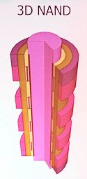
Jim Handy, the “SSD Guy” and the “Memory Guy,” just published a short blog post alerting us to the fact that Flash memory maker SK Hynix has entered the SSD market just four days after announcing the purchase of Link_A_Media, an SSD controller and hard-drive read-channel chip vendor. (See “SK Hynix to acquire SSD controller vendor Link_A_Media for $248 million. That makes four.”) The company lists two types of SSDs on its site: a 2.5-inch drive that transfers data at 6Gbps and mSATA drives that transfer data at 3 or 6Gbps. The 2.5-inch drive is available in capacitirs of 128 and 256Gbytes and the mSATA drives are available in capacities of 32 to 128Gbytes. All drives consume less than 1W in active more and approximately a quarter of a Watt in idle mode.

Significantly, all of the SK Hynix SSDs support 128-bit AES encryption/decryption.

The performance of these SSDs looks pretty impressive from the charts:

There are a couple of significant things we know about the internals of these drives based on Handy’s writeup. First, the drives are based on ONFi Flash memory, which is mucho fast. SK Hynix makes ONFi Flash memory, which should not be much of a surprise.

Second, I guess we now know why SK Hynix bought Link_A_Media. Just refer back to the performance charts above.

One other aspect of this announcement that interests me is that SK Hynix has been placing bets on non-volatile semiconductor memory technologies that might or might not supplant Flash memory sometime in the future. Just this month, the company announced a partnership with IBM to commercialize phase-change memory (PCM, also called PCRAM). That announcement came on the heels of a joint MRAM development agreement between SK Hynix and Toshiba that was announced less than a year ago and an announcement in 2010 that SK Hynix and HP would jointly work to commercialize memristor-based memory. After all, you don’t have to make an SSD out of NAND Flash memory if there are better alternatives to be had.

This move up the food chain by SK Hynix is a significant announcement and one sure to get the attention of the other NAND Flash memory vendors as well as SSD vendors.

Posted in Flash, mSATA, ONFI, SATA, SSD, Storage | Tagged , , , , , | Leave a comment

Registration opens for the Flash Memory Summit 2012. Read on for program highlights

The Flash Memory Summit takes place on August 21-23 here in Silicon Valley at the Santa Clara Convention Center and it’s now opened its registration. However, before you register, you might want to know what’s being covered. A reasonable request and one now easily answered:

  • Pre-Conference (Monday) events: Seminar on Solid State Drives – The Fundamentals
  • Tuesday Morning tutorials: Flash Memory in Data Centers, Flash Memory-Based Architectures, Enterprise Solid State Drives (SSDs)
  • Tuesday Afternoon tutorials: Enterprise Storage Design, Flash Memory-Based Architectures (continued), SSD Technology, NVMe (new standard for PCIe-based SSDs)
  • Wednesday Morning tutorials: Controllers and Flash Memory, Enterprise Caching, Testing/Performance/Endurance, Enterprise Applications
  • Wednesday Afternoon tutorials: Controllers and Flash Memory (continued), Flash and Virtualization, Enterprise Applications (continued)
  • Thursday Morning tutorials: Client Caching, Enterprise Applications (continued)

The Program is here.

Register here.

Posted in Flash, SSD | Tagged , | Leave a comment

SSD prices: More affordable? Steady, substantial decline? In free fall? Just what is going on here?

Senior Writer Vincent Chang over at CNET writes that “SSDs are more affordable than ever” and has the charted data to prove it. Clayton Vallabhan at ITPnet.com goes even further, writing “SSD prices in freefall.” For an even more extensive technical analysis of the decline in SSD pricing, see “SSD prices in steady, substantial decline” by Geoff Gasior on the TechReport.com Web site.

To get a handle on things, I turned to my go-to guy on Flash memory, Jim Handy of Objective Analysis, who writes two blogs you might want to follow if you’re interested in memory. The first is called “The SSD Guy” and the other is called “The Memory Guy.”

Earlier this month, Handy wrote about NAND Flash memory pricing in “The Memory Guy” blog. He started the blog with this:

“Last January at the Storage Visions Conference in Las Vegas (held every year just prior to CES) I asked the audience what they would do when NAND flash reached a price of 35¢ per gigabyte.  My projection (the dotted red line on the chart at left) was that prices would reach that level by the end of the year.

My audience was shocked to hear such a low price!”

Here’s the chart Handy projected:

Then Handy wrote:

“Well, I was wrong – according to spot-market watcher InSpectrum NAND chip prices have already reached that level (the black line on the chart.)  A competing firm, DRAMexchange claims that chip prices are no lower than 41¢/GB, but that microSD cards are going for as little as 29.5¢/GB.

How low can prices go?  Objective Analysis‘ cost model estimates that to reach 35¢/GB a manufacturer would either need to be using a 24nm (or smaller) process to manufacture TLC flash or a 20nm (or smaller) process with MLC.  Given that the market acceptance of TLC has been relatively low outside of SanDisk this puts a lot of pressure on NAND flash makers whose processes are not all that aggressive.”

So as you can see, NAND Flash prices have been falling faster than analysts like Jim Handy expected and the pricing drop is certainly being reflected in the price of SSDs, where the major component cost is indeed the NAND Flash memory chips.

By the way, Handy will be at Memcon in September. If you have a question to ask him and it needs to be in person, you’ll find him there.

Posted in Flash, NAND, SSD, Storage | Tagged , , , | Leave a comment

Samsung’s 20nm-class DDR3 SDRAM runs on 1.35V, saves 2/3 of the power used by 50nm-class, 1.5V SDRAM

Not all DDR3 SDRAM is created equal. That’s the message Samsung is spreading lately by talking about its 20nm-class DDR3 SDRAM. The company is using 1.5V, 50nm-class DDR3 SDRAM as a benchmark and says that a server loaded with 96Mbytes of the 1.5V DDR3 SDRAM consumes 65.3W just in the DRAM. Multiply that by the tens of thousands of servers in a data center and you’ll quickly realize that the energy and cooling costs just for the DRAM are significant. Compare that with the 21.8W that Samsung claims is consumed by its 1.35V, 20nm-class DDR3 SDRAM. There’s a 67% difference in power consumption there, but it’s not just a result of the lower operating voltage because the 30nm-class DDR3 SDRAM also runs at 1.35V and consumes 33.6W—about a third more.

Why? According to this article in The Register, “The paths traversed by the electrons in the smaller process chips are shorter, so less energy is needed to push them around the chips.” That was said by Samsung Semiconductor Europe GmBH’s Peyman Blumstengel, a senior manager for strategic business development. In tech speak, I’d say that the lower impedances of the shorter on-chip traces permit the use of lower-power I/O drivers.

Lots more numbers and figures on Samsung’s site, here. Oh, and I think this will be a topic of discussion at Memcon in September. You can sign up over there on the right side of this blog.

Posted in DDR3, DRAM, SDRAM | Tagged , , , | 1 Comment

Briefly noted: Greenliant adds 8, 16, and 32Gbyte e.MMC SSDs

Yesterday, Greenliant announced that it was adding SSDs to its NANDrive product line in the e.MMC form factor. These new drives are available in 8, 16, and 32Gbyte capacities and complement the SATA and PATA drives already in the NANDrive series. The e.MMC NANDrives are package in 100-ball BGAs and measure 14x18mm.

Posted in Uncategorized | Leave a comment

SK Hynix to acquire SSD controller vendor Link_A_Media for $248 million. That makes four.

Memory Industry Analyst Jim Handy took the unusual step of sending out an alert yesterday. The topic of the alert was the announced acquisition of Link_A_Media Devices (LAMD) by SK Hynix for a reported US $248 million. LAMD is a long-time supplier of read-channel chips but the SK Hynix press release only discusses LAMD’s relatively new foray into NAND Flash controller chips: “Upon completion of the acquisition, LAMD will join SK Hynix as a business unit focused on customized NAND based solutions.”

Very recently, Corsair announced an SSD with one of those LAMD NAND Flash controllers inside. (See “Corsair does the Neutron dance with new line of fast SSDs based on Toggle NAND Flash”) The controller chip in the Corasir Neutron SSD is the LM87800 SSD controller from Link_A_Media.

SK Hynix has also been in the news a lot lately as noted in this blog post from the Denali Memory Report: “SK Hynix places bet on third wannabe non-volatile memory technology, phase-change memory, with IBM.” It appears that SK Hynix is playing a lot of cards on acquiring the technologies needed for future SSD manufacturing.

Referring back to Handy’s alert:

“This is the fourth SSD controller company to be acquired recently:

  • In March of last year OCZ acquired Indilinx
  • LSI acquired SandForce in October
  • December brought Apple’s acquisition of Anobit
  • Now SK Hynix has acquired Link_A_Media

The SandForce and Anobit acquisitions were explored blog post in Handy’s blog The SSD Guy

Posted in SSD, Storage | Tagged , , | 1 Comment

Briefly Noted: JEDEC publishes “A” rev of UFS HCI standard

JEDEC announced today that it has just published an “A” revision of the spec (JESD223A) for the Universal Flash Storage Host Controller Interface (UFS HCI), a companion to the JESD220 standard for UFS, a Flash storage specification for a range of mobile devices including smartphones, digital cameras, and possibly tablets. UFS is widely seen as the eventual successor to the highly successful series of SD cards, bringing more capacity and more bandwidth to portable storage.

If you’re a JEDEC member, you can download the JESD223A standard now at the JEDEC site (www.jedec.org). It’s also available for purchase.

For more information, see Richard Goering’s Industry Insights blog post “Seven Emerging Mobile Device Standards – and How to Verify Them”.

Posted in JEDEC, UFS | Leave a comment

Will cache SSDs rule the world in notebook storage? IHS iSuppli’s Magic 8 Ball says “Signs point to Yes”

An excellent article by Hot Hardware’s Joel Hruska (see “Analysts Predict Skyrocketing SSD, Cache Drive Sales, But What Happened To Hybrid Hard Drives?”) contains several tasty bits of data and a quote from Ryan Chien, analyst for memory and storage at HIS iSuppli. First and foremost is the prediction that sales of cache SSDs, which are SSDs used strictly to cache HDDs, will grow explosively in 2012 and 2013. Here’s the graph from the IHS iSuppli press release:

According to the definition in the IHS iSuppli press release, “cache SSDs are employed as a discrete, separate memory component alongside a hard disk drive, with both elements existing side by side, not together in one housing unit.” The reason that IHS iSuppli believes that cache SSDs will ship in significantly larger volumes that hybrid HDD/SSDs (drives that combine an HDD and Flash in one physical package) is because each hybrid drive is a proprietary design. From Hruska’s article: “… hybrid hard drives are less popular due to single-source manufacturing (Seagate has the only solution on the market) and a lack of options.” So despite the advantage in physical volume, hybrid HDD/SSDs suffer from lack of interchangeability–especially right now because they are currently single-sourced. Notebook PC vendors have many more options with cache SSDs, .

At the same time, all-SSD approaches to notebook storage still prove too expensive when measured using a cost/Gbyte metric. From the IHS iSuppli press release quoting Chien: “The cache SSD solution was first hit upon by PC manufacturers because the use of a dedicated solid state drive proved too expensive when passed on to consumers in the retail market.”

For the full IHS iSuppli press release on this topic, see “Cache is King in Solid State Drive Market.”

If you would like to ask the Magic 8 Ball a question, click here.

Posted in Flash, HDD, SSD, Storage | Tagged , , , , , , | Leave a comment

Violin Memory’s Narayan Venkat writes about why Flash-based storage is doing well in data centers: time and money

Narayan Venkat, VP of product management at Violin Memory, recently published a guest blog post titled “6 Reasons Solid State Memory Is The Biggest Story In Computing” over at Forbes.com. The rhetoric in the article should be familiar stuff to regular readers here at the Denali Memory Report but Venkat makes a few new points about why he believes that Flash-based storage is faring better in data centers than in notebooks and other portable devices and he has a few perspectives worth discussing here. Venkat’s six reasons are:

  • Latency
  • Technology
  • Inertia and The Innovator’s Dilemma
  • Energy
  • Big Data
  • Volume Economics

I’ll comment on just two of these reasons and let you decide about the other four:

For latency, Venkat’s point is that time equals money in a corporate setting and nowhere is this equation more prevalent than in equities and futures trading. Microseconds lost mean millions of dollars lost, an equation that spans a 12-decade range. If Flash-based storage can give an edge in latency (and it does) then there’s a real dollar value that can be placed on it. If Flash-based storage vendors put together the right value proposition, it’s easy to see if it makes business sense or not.

Energy costs at some data centers now consume 30% or more of the centers’ operating budgets. If Flash-based storage can reduce energy consumption relative to high-RPM, short-stroke hard drives (and it does), then there’s another hard dollar cost that can be attributed to the asset side of the ledger for Flash-based storage.

Posted in Flash, SSD, Storage | Tagged , , , | 4 Comments

SK Hynix places bet on third wannabe non-volatile memory technology, phase-change memory, with IBM

When I was really young, I used to play a card game called “Pit” where you tried to corner the market on a particular commodity like oranges, sugar, soybeans, or corn. The game was based on the trading pits of the commodities exchanges and the goal is to get as many people as possible screaming for commodities trades. (Parker Brothers still offers the 98-year-old card game and you can get a copy from Amazon for $6.99.)

What does this have to do with memory? It looks to me as though SK Hynix is playing its own version of Pit with respect to non-volatile memory. The company just announced a partnership with IBM to commercialize phase-change memory (PCM, also called PCRAM). That announcement comes on the heels of a joint MRAM development agreement with Toshiba announced less than a year ago and an announcement in 2010 that SK Hynix and HP on joint work to commercialize memristor-based memory.

According to most market-share analysis reports on the Web (including this one from weSRCH), SK Hynix is the number four vendor of Flash memory in the world after Samsung, Toshiba, and Micron. It looks like SK Hynix is determined to become the leader in the successor to NAND Flash memory, no matter what that technology will be.

Posted in Hynix, Memristor, MRAM, NAND, PCM | Tagged , , , , , , , , , , | 2 Comments

Want a quick and dirty overview of the new JEDEC LPDDR3 spec? EETimes serves it up

Kristin Lewotsky has just published an LPDDR3 SDRAM interview with Huong Vuong, Chairman of the JEDEC JC-42.6 Subcommittee for Low Power Memories. Here are the salient points from the interview, in my opinion:

  • The purpose of LPDDR3 is to increase LPDDR2 performance from 1066Mbps to 1600Mbps with minimal changes to the aging LPDDR2 spec
  • Two key additions made to the spec are write leveling and C/A (command/address) training
  • LPDDR3 also lowers the I/O capacitance limit to improve timing
  • Work has already started on the LPDDR3E spec that will increase memory bandwidth and the LPDDR4 spec with the intent of doubling LPDDR3 performance

Write leveling and C/A training allow SDRAM memory controllers to compensate for signal skew between the controlling SoC and the LPDDR3 SDRAM, which helps to ensure that data input setup and hold times and command/address input timing requirements are met at these higher transfer rates.

Note: For a quick bring-me-up-to-speed tutorial on LPDDR2, see “LPDDR2: The new mainstream memory for embedded and mobile applications?” and “State-of-the-Art in Low-Power Memory: Denali’s MemCon”.

Posted in LPDDR2, LPDDR3, LPDDR3E, LPDDR4, SDRAM | Tagged , , , , , , | Leave a comment

Yes Virginia, there was a Denali Party at DAC. “Nobody” came

Photo: Joe Hupcey III, Cadence

Yes, there was a Denali Party at DAC 2012, sponsored by Cadence. It was held at the Ruby Skye nightclub, the same place it was held last time DAC rolled into San Francisco.

“Nobody” came to the party, like the person over there on the right.

“Nobody” danced. “Nobody” drank.

“Nobody” stayed up after midnight.

And “Nobody” dragged into DAC the next day with a hangover.

Here’s a photo of a bunch more “nobodies” enjoying themselves at the event:

Photo: Joe Hupcey III, Cadence

Posted in Uncategorized | Tagged , , | Leave a comment

Flash Memory Summit 2012, Santa Clara, CA. Registration now open

Every year, the Flash Memory Summit rolls into Silicon Valley to discuss the latest in Flash memory, SSDs, and possibly up-and-coming alternative non-volatile memory technologies. This year, the event takes place on August 21-23 at the Santa Clara Convention Center in the center of Silicon Valley. It’s too soon to know what the technical program will look like, but the call for presentations includes this list of desired topics:

  • Flash memory (including green Flash)
  • New non-volatile technologies
  • Enterprise storage systems
  • Flash endurance/reliability
  • Solid state drives (SSDs)
  • SSD controllers
  • Security/content protection
  • Standards
  • Flash (USB) disk
  • Hybrid (multilevel) storage systems

You can register here.

Posted in Flash, MRAM, NAND, SSD, Storage | Tagged , | Leave a comment

Corsair does the Neutron dance with new line of fast SSDs based on Toggle NAND Flash

PC hardware maker Corsair has introduced a new line of 2.5-inch, 7mm SSDs called the Neutron GTX series. I find it very interesting that the first fact put forth in the Corsair press release for this new series is about the Flash media controller in the drive. The controller chip is the LM87800 SSD controller from Link_A_Media, an 8-year-old Silicon Valley startup company. This Corsair announcement is yet another indication of how important the controller is in SSD design. It’s so important that it’s a significant differentiator in terms of the performance realized by the SSD. The Neutron GTX drives employ high-speed Toggle NAND Flash to support the controller’s speed and together, they support the drives’ 6Gbits/sec SATA interface.

The Neutron GTX SSD series delivers 555Mbytes/sec read and 500Mbytes/sec write operations and up to 90,000 random read and write IOPs (input/output operations per second), which greatly speed data-intensive tasks like video and image editing. Drive capacities range from 120 to 480Gbytes.

According to the press release, the Corsair Neutron GTX drives will be available next month.

Posted in Flash, NAND, SSD, Toggle | Tagged , , | Leave a comment

So just how big is the semiconductor memory market? $50 billion? $60 billion?

Yesterday, Jeremy Wagstaff, Chief Technology Correspondent for Reuters in Asia, published an article on wannabe non-volatile memory technologies such as MRAM and Memristors or ReRAM (See “Pushing the PRAM: when chips just can’t get any smaller”). The lure is a big piece of the semiconductor memory pie. How big a piece? Well, the deckhead in Wagstaff’s article says it’s a $50 billion industry. Deeper in the article, Wagstaff writes that the Flash market was $21 billion last year and that the DRAM market was $30 billion.

By coincidence, I looked over a detailed report on semiconductor memory from research house Databeans yesterday. According to Databeans, memory makes up some 20% of the $300 billion semiconductor market. That works out to about $60 billion.

It’s a big lure, which is why you see all of these wannabe memory fish closing in.

Posted in DRAM, Flash, Memristor, MRAM | Tagged , , , , , | Leave a comment

Denali Memory Report gets a plug in Reuters story

Jeremy Wagstaff has just published an article on the rapidly evolving memory scene though Reuters. The article is titled “Pushing the PRAM: when chips just can’t get any smaller” and it does a good job of painting the current landscape. It mentions Denali Memory Report, by the way.

Posted in Uncategorized | Leave a comment

3D Thursday: Advantest 3D tester produces known good die and known good stacks

3D can’t move forward until the testability issues are solved. Hear that one? Well, Advantest has just advanced another click in that ratchet with this week’s introduction of a concept model test cell for TSV-based 2.5D and 3D products. It’s called DIMENSION and it’s designed for:

  • Delicate and thin die handling
  • Active thermal management
  • Overall yield management

The DIMENSION tester employs a Smart Die Carrier so that the tester can pick and place thin die with fine-pitch contacts. Soft-touch handling is built in to prevent cracking of thinned semiconductor die. Built-in Active Thermal Control permits testing to spec and yield parameters. Together, these innovations permit the tester to produce tested KGD (known good die) and KGS (known good stacks).

Next problem?

Posted in 3D, Wide I/O | Tagged , , , | Leave a comment

Will SSDs be the first big market for 3D NAND Flash memories?

I’ve been meaning to write about a comment regarding NAND Flash memory and SSDs written by Thomas McCormick in LinkedIn’s Solid State Storage Group and this seems like the perfect time. McCormick is an Integrated Hardware/Software Product Development Leader at ECI Innovations, a custom instrumentation and control systems design house in Chelmsford, MA. McCormick was responding to a blog post written by Greg Schulz (“Researchers and marketers don’t agree on future of NAND flash SSD”) who founded Storageio and whose blog is located at storageioblog.com. In the post in question, Schulz discussed the famous/infamous UCSD report on the bleak future of NAND Flash memory. (For even more details, see my discussion of that report at “The sky is falling! The sky is falling! Paper predicts the bleak future of SSDs and NAND Flash memory”)

Essentially, the UCSD paper concluded that NAND Flash memory optimized for simpler applications such as USB memory drives and SD cards emphasizes cost/bit over durability, reliability, and retention time, thus making such NAND Flash memory increasingly unattractive for use in SSDs, which need to emphasize the attributes that aren’t presently valued.

In his comment to the Schulz blog post, McCormick wrote:

“I think that there is little doubt that NAND flash market has been predominantly chasing $/GB. All other parameters such as endurance, performance, retention, BER appear to be secondary concerns as they have been degrading rapidly with recent NAND process technologies (both shrink and increasing bits per cell).

Flash memory system designers serving markets other than consumer (such as enterprise and embedded) need to be concerned with these diminishing parameters and design flash memory systems that make accommodates for these new parameters. Researchers can point out the flaws, but researchers can also develop solutions as can flash system designers in industry. There is always another replacement technology for NAND just around the corner, but the present is NAND and researchers and industry need to work together to ensure that the needs of the markets are met.”

When I wrote about the UCSD report, I discussed alternative storage media such as MRAM and Memristors, which both aspire to the non-volatile memory crown currently worn by NAND Flash memory. But McCormick’s comment suggested yet another alternative, which is why I’ve returned to this topic.

It’s entirely possible for the NAND Flash industry to niche itself the way that the DRAM market has become niched. For DRAMs, we now have part families optimized for PCs and Servers (DDR), for mobile applications (LPDDR), and for graphics (GDDR). If SSDs get big enough—and there’s no reason to doubt that they will if they haven’t already done so—then there’s a possibility that a new niche for NAND Flash memory could arise with somewhat different optimizations than those employed for the USB memory stick and SD card markets. In fact, the promises of improved durability and reliability of 3D NAND Flash memory might well be first realized in parts optimized for SSD applications.

Posted in 3D, DDR, DRAM, Flash, Memristor, MRAM, NAND, SSD, Storage | Tagged , , , , , , , | Leave a comment

Toshiba launches family of thin 2.5-inch and mSATA SSDs based on 19nm Toggle NAND Flash

Toshiba has just launched a new SSD family called the THNSNF series based on the company’s 19nm Toggle NAND Flash multi-level cell (MLC) devices. The SSDs are offered in capacities from 64 to 512Gbytes. All members of the family employ 6Gbps SATA interfaces. Member of this family include 9.5mm and 7mm 2.5-inch drives and three mSATA drives in capacities from 64 to 256Gbytes. The press release mentions the use of a Toshiba-proprietary error-correction code called “Quadruple Swing-By Code” or QSBC. Error correction is a major point of SSD differentiation and it appears that Toshiba has something new here to talk about.

The THNSNF press release also says something about “efficient power utilization of less than 0.1W” but the preliminary data sheet makes no mention of power consumption. If the press release power numbers prove out, then these drives are going to become mighty popular in notebook computers, tablets, and many other portable devices. For comparison, Toshiba’s new THNSNS SSDs based on 24nm NAND Flash devices draw between 3.7W and 5.8W depending on capacity.

The new THNSNF drives are expected to be available in August.

Posted in mSATA, SATA, SSD, Toggle | Tagged , , | Leave a comment

DRAMeXchange tests this year’s crop of 120Gbyte SSDs. Guess which one wins…

Yesterday, DRAMeXchange published some performance tests on five 120Gbyte SSDs. The results may surprise you. Click here:

DRAMeXchange’s 2012 SSD Ranking – 120 GB SSD (SATA 2)


Posted in SSD | Tagged | Leave a comment

MRAM spotted in Buffalo Memory SSD—for cache

Several sources including TomsHardware.com have reported the appearance at the 15th Embedded Systems Expo in Japan of an SSD built by Buffalo Memory Company with MRAM for cache memory. The drive uses 8Mbytes of MRAM (magnetic RAM) as a cache for the much larger Flash storage array and the nonvolatile nature of the MRAM gives the drive more protection from power loss. All of the articles about this product suggest that the drive has an overall capacity of 4Gbytes, but that seems unlikely in a new product considering the state of Flash manufacturing and the sizes of competing SSDs. We’ll have to wait to see what the final drive looks like because Buffalo has not yet announced the product formally.

Posted in Flash, MRAM, SSD | Tagged , , , | 1 Comment

This SSD will self destruct…immediately. On Command (See the video)

In case you need an SSD that can be wiped quickly, RunCore has introduced the InVincible SSD with two modes of erasure: non-destructive and destructive. Two buttons—one red, one green—activate the erasure. The two buttons apparently connect to the SSD’s normal SATA drive connector. The green button simply erases the drive’s internal Flash memory. For really sensitive data, the red button applies excessive voltage to the Flash memory letting out the magic smoke (seen in the video below) and this preventing the drive from ever working again.

Here’s the video:

Postscript: the SSD on my laptop failed catastrophically just yesterday. Maybe I shouldn’t have written up this particular story for the Denali Memory Report.

Posted in SSD | Tagged , , , , | 2 Comments

DFI 3.1 spec adds DDR4 and LPDDR3 coverage for speed and low-power benefits

Earlier this month, JEDEC published the LPDDR3 specification for the next generation of low-power SDRAM that will be used in mobile devices such as smartphones, tablets, ultra-thin notebooks and similar connected devices on the newest, high-speed 4G networks. The LPDDR3 supports memory transfer rates of 6.4Gbits/sec—12.8Gbits/sec for a dual-channel configuration—and the DDR4 spec support memory transfer rates of 3.2Gbits/sec per pin. Now, the DDR PHY Interface (DFI) Group has announced a revision of the DFI specification (version 3.1) that adds LPDDR3 and DDR4 capabilities to the existing specification. The DFI spec defines a standard interface between DDR memory controllers and the PHYs that communicate directly with the associated SDRAM chips.

Coincident with the DFI announcement, Cadence has announced DDR controller and DDR PHY design IP and verification IP that conforms to the DFI and JEDEC specifications.

Posted in DDR, DDR4, DFI, JEDEC, LPDDR3 | Tagged , , , , | Leave a comment

Invensas to detail POP interconnect to rival Wide I/O with as many as 1200 interconnections between IC packages

Later this week, Invensas will detail its new BVA (bond via array) package-on-package (POP) interconnect that can achieve 1200 electrical connections between chip packages without the use of 3D die assembly. Information on the technology will be contained in a paper titled “Fine Pitch Copper PoP for Mobile Applications” to be given during the 3D Technology session (June 1) at the Electronic Components and Technology Conference (ECTC) at the Sheraton San Diego Hotel and Marina in San Diego.

The Invensas press release claims that the company’s BVA technology permits as many as 1200 interconnections between packages using conventional POP assembly techniques using an interconnect pitch as small as 0.2mm. Because it is a POP technology, Invensas also claims that its BVA technology extends the life of the existing package assembly and SMT infrastructure.

Posted in 3D, Wide I/O | Tagged , , , | Leave a comment

The Denali Memory Report is on vacation and will return on May 26, 2012

Posted in Uncategorized | Leave a comment

Semiconductor memory plays a large role in smartphone design says Matti Floman of Nokia

“There’s no real difference between PCs and mobile phones today,” said Matti Floman from Nokia who gave the first keynote speech at last week’s JEDEC Mobile Forum. There is no difference in the types of applications run; there’s no difference in performance; there’s no difference in connectivity. Because smartphones now offer the sort of universal, run-any-app abilities of PCs, they are rapidly moving down the phone hierarchy, penetrating the broad mobile phone subscriber market and pushing out phones with lesser abilities such as feature phones.

Although user expectations are not different between PCs and phones, there’s certainly a difference in terms of hardware design. It’s not easy to make powerful memory that doesn’t consume lots of power, said Floman. In addition, phones need to fit more and more memory capacity into smaller and smaller volumes to make room for more battery in the phone—to accommodate users’ desire for more time between battery charges. Smartphone form factors are also evolving, said Floman. The favored form factor these days is a thin phone with a large display.

Semiconductor memory requirements to accommodate these design characteristics include:

  • Scalability (in terms of capacity, performance, and functionality), because no one can see five years ahead
  • More bandwidth
  • New packages (to accommodate 3D IC assembly and thermal issues)
  • Lower power consumption
  • Scalable modules
  • Standards

Then Floman focused on what’s really important now: power. “Power is the focus of the future,” he said. Power consumption is limited by battery capacity and the heat tolerance of stacked packages, because whether or not the mobile phone makers are using 3D IC assembly, they are already stacking die. Here’s an image Floman used to show the evolution of 3D stacking in smartphone design.

Floman noted that the maximum operating temperature for NAND Flash devices is 85° C and that DRAMs are limited to 105° C. Die stacking compounds the problem of heat dissipation.

One of the most interesting slides that Floman presented at the JEDEC Mobile Forum, in my opinion, was an image that showed three processor/memory architectures for mobile phones. The graphic looked like this:

The two architectures on the left are execute-in-place (XIP) architectures. The leftmost architecture employs pseudo-static RAM and NOR Flash as memory and executes operating-system code directly from the NOR Flash memory. The middle architecture replaces the pseudo-static RAM and NOR Flash memory with LPDDR2 SDRAM and LPDDR2-N Non-Volatile Flash memory. It’s still an execute-in-place architecture but the memory components are newer and deliver more performance with better capacity.

The architecture on the right is a shadowing architecture where the OS code is stored in a mass-storage device (NAND Flash memory) and the code is first transferred to DRAM and then executed. High-end smartphones use this architecture.

These architectural designs will hold unless a new type of memory with both fast read/write times and non-volatile storage become commercially available in the required capacities and the required cost per bit. If that happens, the smartphone will only need one memory type—perhaps that might be magnetic RAM (MRAM) or Memristor-based memory. But that’s not the situation today.

The best possible performance, said Floman, will come from Wide I/O DRAM while the UFS (Universal Flash Storage) standard appears to be poised to become the next commonly used storage medium for smartphone design. UFS “will be the next generation mass memory” for smartphones, said Floman.

All of this evolution has but a single purpose. “You will not buy your next phone from the same manufacturer unless it provides new functions,” Floman said as he concluded his keynote speech.

Posted in 3D, DDR, LPDDR2, Memristor, MRAM, SDRAM, Storage, UFS | Tagged , , , , , | Leave a comment

NVM Express (NVMe) controller subsystem points the way to an SSD future

Cadence introduced an NVM Express (NVMe) controller subsystem this week. The Denali Memory Report and the EDA360 Insider have covered NVMe developments several times already (see below for the links) and it’s clear that one way to maximize SSD performance is to connect the SSD to the host CPU through a non-limiting interface. Enter NVMe, which layers storage-centric protocols on the hugely successful and very fast PCIe interface.

The following diagram shows the relationship among the elements of the Cadence NVMe subsystem, which appears in the lower left quadrant of the image:

An NVMe controller implements the storage-centric NVMe commands in the subsystem and passes the resulting command and data streams to a PCIe controller for further formatting. The resulting data stream goes out over the PCIe PHY and data returns through the reverse path. Appropriate firmware manages the overall operation.

Why not combine the NVMe and PCIe controllers into one block? That question goes to the heart of IP-centric design and good practice for IP reuse. The NVMe specification leverages the well established PCIe protocol for its transport layer and the Cadence NVMe subsystem implements that transport layer with a proven PCIe controller and PHY. The subsystem integrates the NVMe controller with the existing PCIe hardware in the same way that the NVMe specification integrates the NVMe layer with PCIe. The Cadence NVMe subsystem also includes Verification IP to aid in system integration.

For more information on this subsystem, see Richard Goering’s blog post titled “How IP Subsystem Will Speed NVM Express (NVMe) Adoption” in his Industry Insights blog.

For more information on NVMe, see the following blog posts in the Denali Memory Report and the EDA360 Insider:

Posted in NVM Express, SSD | Tagged , , , , | Leave a comment

It’s Official: Microsoft joins 3D Hybrid Memory Cube Consortium with Micron, Samsung, Altera, IBM, Open-Silicon, and Xilinx

Last week, the Hybrid Memory Cube Consortium announced that Microsoft had joined Micron, Samsung, Altera, IBM, Open-Silicon, and Xilinx in the development of high-performance 3D SDRAM subsystems based on the Hybrid Memory Cube.

For more information on the Hybrid Memory Cube, see:

Posted in 3D, DRAM, HMC, Hybrid Memory Cube | Tagged , , , , , , , | Leave a comment

SSD Review: Intel 910 PCIe SSD a “game changer”

It’s always great fun to see a company hit one out of the ballpark with a new product and that’s exactly what Intel has done with its new 910 PCIe SSD, if you believe this recent article by Paul Alcorn in SSD Review. In fact, the SSD Review article clearly states:

“If you have any doubt that the Intel 910 Series PCIe SSD is anything less than a game changer, we are certain this will fade throughout reading of this report.”

I discussed the introduction of this Intel SSD product last month in a previous Denali Memory Report blog: “Intel jumps on the PCIe SSD bandwagon with the fast, new 910 Series.” Now, SSD Review has been kind enough to thoroughly document a technical evaluation of the offering and the article’s author is clearly impressed.

Before jumping into the review, I think you should consider the importance of a PCIe-based SSD. One of the chief advantages that SSDs have over HDDs is read speed, thanks to solid-state storage. Forcing SSDs to communicate with host CPUs using a drive interface that’s evolved over decades in service to HDDs adds unneeded latency, as noted in the SSD Review article:

“The PCIe SSD is by far physically one of the easiest ways to integrate flash storage into the server. The form factor is key, with no cabling or connections to other components involved, and the NAND is as close to the CPU as possible. By applying the benefits of the PCIe interface, virtually a ‘straight shot’ to the CPU with current generation chipsets, latencies can be kept as close to DRAM levels as possible.”

In my previous blog, I was able to provide a generic block diagram of the Intel 910 PCIe SSD:

Intel 910 PCIe SSD Block Diagram

Thanks to the SSD Review article, we now know that the PCIe-to-SAS bridge chip is an LSISAS2008 PCI Express to 8-port SAS/SATA controller and that the four “SAS/NAND ASICs” are EW29AA31AA1 SSD controllers jointly developed by Intel and Hitachi. The SSD controller chips can also be found in Hitachi’s Ultrastar Enterprise SAS SSDs. The 400Gbyte version of the Intel 910 PCIe SSD uses two of these SAS SSD controllers and the 800Gbyte version uses four controllers.

Combining this controller technology with high-endurance MLC NAND results in outstanding performance and endurance specifications: 1-2 Gbytes/sec reads, 0.75-1 Gbytes/sec writes, and ten full drive writes per day for five years (a 30x improvement over standard Intel MLC offerings). The MSRP for the 400Gbyte version of the Intel 910 PCIe SSD is $1929 and the 800Gbyte version is $3859. That’s less than $5/Gbyte and is extremely aggressive for an enterprise-class SSD.

The SSD Review article is very thorough and you might well want to spend considerable time with it because it provides an unusual amount of insight into the design of the Intel 910 PCIe SSD. After studying this article, you might well be convinced that PCIe SSDs and the soon-to-be-seen NVMe SSDs that will follow may well be the shape of things to come.

Posted in NVM Express, PCIe, SSD, Storage | Tagged , , , , , , | Leave a comment

Micron samples DDR4 module at 2400Mtransfers/sec. Production pegged in 2013

Micron has begun sampling a DDR4 SDRAM module, which the company has said will lead the way to DDR4 availability in production equipment starting in 2013. The memory chips on the Micron DDR4 module are 30nm, 4Gbit, x8 parts operating at 2400Mtransfers/sec. Micron and Nanya developed the SDRAM chip together. Eventually, Micron expects to raise the DDR4 SDRAM chip’s transfer rate to the JEDEC-defined 3200Mtransfers/sec speed limit.

Micron’s announcement says that the SDRAM chip will be in volume production by 4Q 2102 and predicts that the company will be offering modules based on this DDR4 SDRAM chip in the following form factors:

  • RDIMM
  • LRDIMM
  • 3D
  • SODIMM
  • UDIMM
Posted in DDR4, DRAM, JEDEC, SDRAM | Tagged , , , , , , | 2 Comments

Second Speedy SAS SSD Shows at STA (SCSI Trade Association). Tomorrow

Seagate has become the second company to announce that it will be showing its Pulsar.2 12Gbps SATA SSD at tomorrow’s SCSI Trade Association meeting in Santa Clara, California. The first was Western Digital. (See “WD’s HGST to demo 12Gbps SAS SSD at SCSI Trade Association Technology Showcase next week in California”) Like WD’s announcement last week, Seagate’s press release says its new SSD is compatible with controllers from PMC-Sierra and LSI Corp.

It’s no surprise that the drive vendors are chomping at the bit to up the interface bit rate on SSDs. The interface port is the bottleneck. Internally, SSDs can increase the number of Flash memory channels to get just about any desired bandwidth, so the limiting factor becomes the drive interface bandwidth. What’s in the way? Faster SerDes and the ever-present concerns about backwards compatibility. According to the Seagate release, the 12Gbps version of the SAS standard is “currently stable” and the company expects production drives will hit the market in 2013.

SerDes IP blocks have been able to crack 20Gbps for a while now and such data rates are routinely available on current-generation FPGAs. So you should expect that 12Gbps isn’t the end of the line for SAS interface speed boosts. There’s clearly more to come.

Posted in SAS, SATA, SSD, Storage | Tagged , , , , , | Leave a comment

1Tbyte KingMax SSDs spotted on shelves in Japan. ¥119800 ($1500)

Tweaktown is reporting the appearance of 1Tbyte, 2.5-inch KingMax SSDs on retail shelves in Japan with a price of ¥119800 (about $1500). There’s a photo too, in case you don’t believe the words alone.

Tweaktown cites the original information source as EXPreview.com.

Posted in Uncategorized | Leave a comment

Simple three-bar graph explains all the engineering economics of 3D memory you need to know

The January IEEE Spectrum contained an article titled “3-D Chips Grow Up.” The article reproduced a simple Samsung bar graph about the very real advantages of 3D memory interconnect. That graph tells you all you need to know about why there’s a push to get 3D IC assembly off the ground, at least for memory. Bandwidth up 800%. Power consumption down 50%. Real estate on the pcb reduced by 65%. (Thanks to David Thon for the tip.)

Posted in 3D, SDRAM | Tagged , | 2 Comments

Tiny RunCore single-chip SSDs cram 8 to 64Gbytes onto small SATA cards that fit anywhere

RunCore has announced a line of small single-chip SSDs in a format that the company calls “Mini DOM” (miniature disk on module). The high-speed SATA SSDs are available with capacities from 8 to 64Gbytes in three form factors: a 7-pin horizontal SATA DOM, a 7-pin vertical SATA DOM, and a 22-pin horizontal SATA DOM. Here’s a photo with the three form factors:

It appears that all of the key electronics including the SATA controller and the NAND Flash memory are contained in one “self-designed” 104-ball FBGA package, which is mounted on the small carrier boards in each of the three circuit board formats. All of the drives are available in a commercial temperature grade (0℃ to 70℃) and an industrial temperature grade (-40℃ to 85℃).

Posted in Flash, NAND, SATA, SSD, Storage | Tagged , , , , , | Leave a comment

WD’s HGST to demo 12Gbps SAS SSD at SCSI Trade Association Technology Showcase next week in California

HGST, the Western Digital subsidiary formerly known as Hitachi Global Storage Technologies, has announced a new 12Gbps SAS SSD and will be demonstrating it at the SCSI Trade Association Technology Showcase next week on May 9 at the Hyatt Hotel in Santa Clara, California. The 12Gbps SAS interface is backward compatible with the 6Gbps SAS standard interface but boosts data throughput to a peak of 4.8Gbytes/sec on the dual-ported HGST SSD. Next week’s interoperability demo will show the HGST drive working with controllers from LSI and PMC-Sierra.

(Note: For more information on the 12Gbps SAS interface, see the Denali Memory Report blog post from last month: “Cadence adds 12Gbps SAS and NVM Express verification IP to its VIP catalog”)

Posted in SAS, SSD, Storage | Tagged , , , , , , , , , | 1 Comment