Last week at the Flash Memory Summit, Dr. Sung Wook Park spoke about memory. No surprise there, but there were several surprises in Park’s presentation. The first surprise popped up in the slide immediately following the keynote presentation’s title slide:
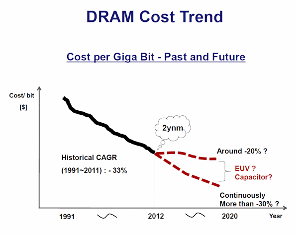
From Park’s perspective, the 33% per year compound annual decline in DRAM cost per bit is about to end at the low 20nm side of the scaling equation (2ynm in the slide). After that, there are some pretty large scaling problems to be overcome and Park didn’t sound optimistic about overcoming them. The reason for his pessimism appeared on the very next slide:
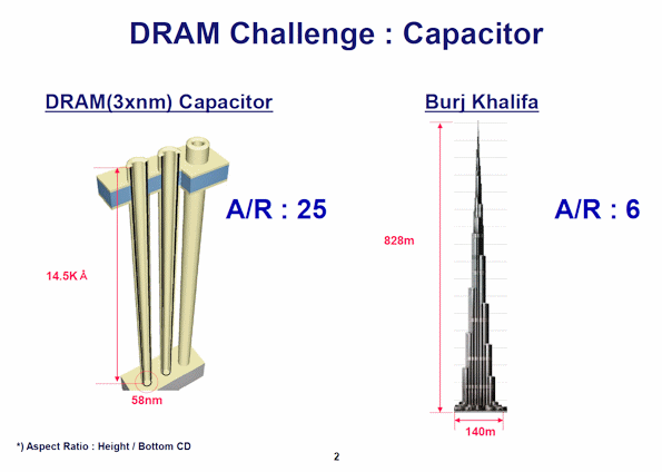
The aspect ratio of the deep capacitors used to store digital bits as charge in DRAMs has gotten ludicrous. The capacitor’s aspect ratio is now at 25. The aspect ratio of the Burj Khalifa, which is currently the tallest human artifact in the world, is only 6. The current capacitor design needs re-engineering or DRAM scaling’s going to slow down significantly.
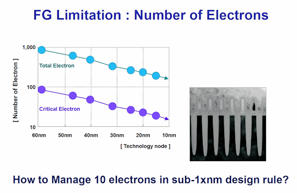
NAND Flash is also running into trouble, in the form of the dwindling number of electrons stored in the NAND Flash cell’s floating gate as the gate’s volume shrinks with each process node.
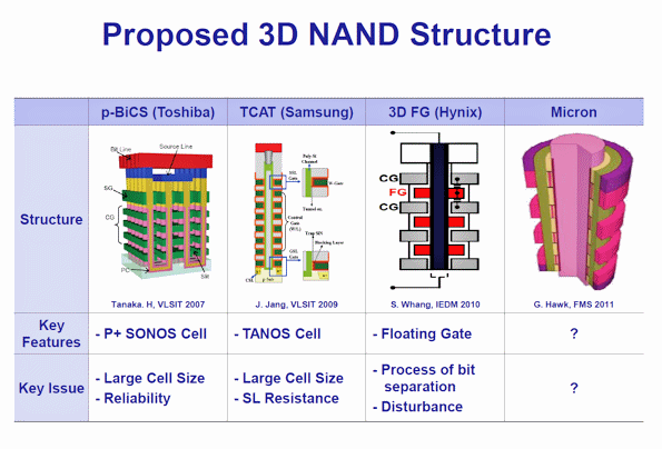
The number of electrons stored in the NAND Flash cell’s floating gate is rapidly headed towards a couple of hundred and there’s a signal/noise problem were the leakage loss of even 10 electrons is becoming problematic. Consequently, there’s a quest for developing 3D NAND Flash cell structures, which greatly expand the volumetric capacity of the bit cell’s floating gate. Park showed a slide with four proposed 3D NAND cell designs from Toshiba, Samsung, SK hynix, and Micron.
For these reasons, SK hynix (and other semiconductor memory vendors) are ramping their search efforts to find replacement technologies for DRAM and NAND Flash. As I’ve written before (see “SK hynix places bet on third wannabe non-volatile memory technology, phase-change memory, with IBM”), SK hynix is pursuing Phase-Change Memory (PCM) with IBM, MRAM (magnetic RAM) with Toshiba, and memristors (resistive RAM or ReRAM) with HP.
Park said that any such memory replacement technology must satisfy at least one of the following:
- Drop-in replacement (pin-for-pin compatible)
- Better cost and power than DRAM.
- Better reliability and performance than NAND Flash memory.
Whatever the replacement memory technology turns out to be, said Park, it must also offer byte-level accessibility.
PCM is the most mature at the moment, said Park. It combines the advantages of Flash and DRAM. It’s still expensive. Nevertheless, there’s a successfully manufactured 1Git, PCM 42nm device and a 2xnm PCM cell structure is in development.
Then Park said that MRAM still needs work. Although MRAM is promising because the cell structure is close to the size of a DRAM cell, there are “still many challenges.”
Finally, said Park, memristors are “still a ways away.” “We need a better understanding of the underlying mechanism and its reliability,” he explained.
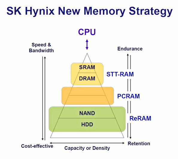
With all of these caveats, one of Park’s final slides showed that SK hynix has found a place for each of these three wannabe memory technologies in a system:
Park’s slide shows SRAM and DRAM being replaced with STT-MRAM (STT stands for “spin-torque transfer). PCM or ReRAM could be a possible replacement for NAND Flash and hard disk drives. PCM (PCRAM) appears to fall into a currently unpopulated memory niche between DRAM and NAND Flash memory. These positions in the memory hierarchy are based on the respective cost, bit-density, and performance characteristics of the prospective memory technologies.
Is this really the future? Who knows? But we do now know where and how SK hynix is placing its bets.
Dr. Park’s Flash Memory Summit 2012 keynote presentation is here.
You can also see Richard Goering’s blog on this topic: “Keynote: New Memory Technologies Challenge NAND Flash and DRAM”



— Finally, said Park, memristors are “still a ways away.” “We need a better understanding of the underlying mechanism and its reliability,” he explained —
Very interesting! What underlying mechanism in case the memristor is a mere hypothetical concept which can never be realized? (“Fundamental Issues and Problems in the Realization of Memristors” (arXiv:1207.7319v1 [cond-mat.mes-hall]))
Memristors, at least the ones within HP’s definition, are not hypothetical. They already have been realized according to HP and to several other published papers. What’s not clear is the precise mechanism for making and breaking the electrical connection within the memory cell. Although the mechanism isn’t clear, what is clear is that the mechanism does work, however it works. Sort of like gravity, which also eludes our explanation. We’re still trying to detect gravitons and gravity waves, but no one is flying off the earth because we’ve not pinned down the mechanism.
HP’s research has shown that – by “electroforming” – a thin TiO2 layer can be brouht into a state where local regions of the layer can be switched between different resistance states by repeated electric stressing. Such a behaviour is well known stuff and occurs very often after the so-called soft breakdown of insulating films (maybe, that’s the reason for the reliability problems as breakdown phenomena generally follow some statistics) . Physically, this resistance switching reminds on local phase changes somewhere in the material triggered by electric stress.
Memristors according to HP’s model definition must be hypothetical as the physics behind this memristor concept seems to be in conflict with fundamentals of irreversible thermodynamics.